

Manufacturing method for high-power-density LED carrier board
A production method and high-power technology, which are applied in circuit substrate materials, printed circuit manufacturing, printed circuits, etc., can solve the problems of strong brittleness of ceramic substrates, not easy to thin, and expensive hole metallization. Good peel strength and satisfactory workability
- Summary
- Abstract
- Description
- Claims
- Application Information
AI Technical Summary
Problems solved by technology
Method used
Image

Examples
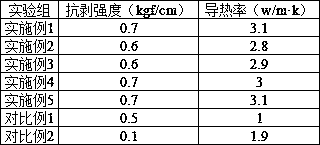
Embodiment 1
[0025] A method for manufacturing a high-power density LED carrier board, characterized in that it includes the following steps: material cutting → drilling → PTH → electroplating → solder resist plug hole → grinding → outer layer circuit → solder resist → surface treatment → post-process; The hole diameter of the hole processed by the drilling process is ≤1000u", the hole position accuracy is ±30um, and the CPK≥1.33.
[0026] Further, the drilling process uses 2 carrier boards / stack. When drilling, a white backing board is set under the carrier board, and a coated aluminum sheet cover board is placed above it.
[0027] Further, in the PTH and electroplating process, the screen plate of the plug hole is 40T, the plug hole is left standing for 3 hours, and pre-baked at 75° C. for 45 minutes, so that the fullness of the plug hole reaches 60%.
[0028] Further, the grinding process requires that the orifice ink should be ground clean, and the copper surface should not have obviou...
Embodiment 2
[0040] A method for manufacturing a high-power density LED carrier board, characterized in that it includes the following steps: material cutting → drilling → PTH → electroplating → solder resist plug hole → grinding → outer layer circuit → solder resist → surface treatment → post-process; The hole diameter of the hole processed by the drilling process is ≤1000u", the hole position accuracy is ±30um, and the CPK≥1.33.
[0041] Further, the drilling process uses 2 carrier boards / stack. When drilling, a white backing board is set under the carrier board, and a coated aluminum sheet cover board is placed above it.
[0042] Further, in the PTH and electroplating process, the screen plate of the plug hole is 30T, the plug hole is rested for 2 hours, and pre-baked at 65° C. for 35 minutes, so that the fullness of the plug hole reaches 40%.
[0043] Further, the grinding process requires that the orifice ink should be ground clean, and the copper surface should not have obvious frost...
Embodiment 3
[0055] A method for manufacturing a high-power density LED carrier board, characterized in that it includes the following steps: material cutting → drilling → PTH → electroplating → solder resist plug hole → grinding → outer layer circuit → solder resist → surface treatment → post-process; The hole diameter of the hole processed by the drilling process is ≤1000u", the hole position accuracy is ±30um, and the CPK≥1.33.
[0056] Further, the drilling process uses 2 carrier boards / stack. When drilling, a white backing board is set under the carrier board, and a coated aluminum sheet cover board is placed above it.
[0057] Further, in the PTH and electroplating process, the screen plate of the plug hole is 50T, the plug hole is rested for 4 hours, and the plug hole is pre-baked for 55 minutes at 80° C., so that the fullness of the plug hole reaches 70%.
[0058] Further, the grinding process requires that the orifice ink should be ground clean, and the copper surface should not h...
PUM
| Property | Measurement | Unit |
|---|---|---|
| Average particle diameter | aaaaa | aaaaa |
| Thermal conductivity | aaaaa | aaaaa |
| Average particle diameter | aaaaa | aaaaa |
Abstract
Description
Claims
Application Information