Array substrate structure, display device and preparation method of array substrate structure

一种阵列基板结构、金属层的技术,应用在电气元件、电固体器件、电路等方向,能够解决TFT器件可靠性难以保证、TFT器件存储电容降低、工艺复杂度提高等问题

Active Publication Date: 2021-07-30
FUJIAN HUAJIACAI CO LTD
View PDF5 Cites 0 Cited by
  • Summary
  • Abstract
  • Description
  • Claims
  • Application Information

AI Technical Summary

Problems solved by technology

However, the continuous reduction of the pixel area will inevitably lead to an increase in the complexity of the process, a continuous reduction in the storage capacity of the TFT device, and even make it difficult to guarantee the reliability of the TFT device.

Method used


Image

  • Array substrate structure, display device and preparation method of array substrate structure
  • Array substrate structure, display device and preparation method of array substrate structure
  • Array substrate structure, display device and preparation method of array substrate structure

Examples


preparation example Construction

[0041] The present invention also provides a method for preparing a TFT array substrate, comprising the following steps:

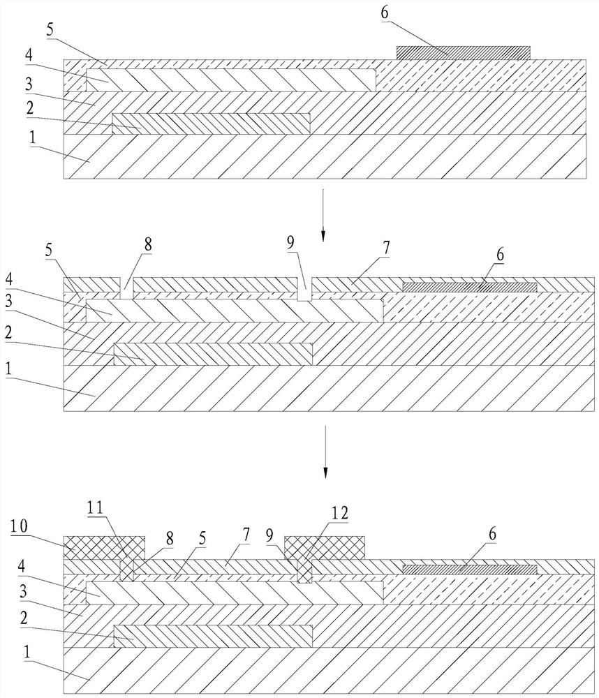
[0042] Step 1: sequentially forming a gate, a gate insulating layer, an active layer and an etching barrier layer on the substrate, the gate being formed by a first metal layer;

[0043]Step 2: forming an auxiliary metal layer on the etching barrier layer;

[0044] Step 3: forming a passivation layer on the etching barrier layer and the auxiliary metal layer;

[0045] Step 4: Simultaneously pattern the passivation layer and the etching barrier layer through a patterning process to form a first via hole and a second via hole connected to the active layer;

[0046] Step 5: forming a third metal layer on the passivation layer, the third metal layer is connected to the active layer through the first via hole and the second via hole; A source electrode and a drain electrode are respectively formed at the first via hole and the second via hole.

[0047] Furth...

Embodiment 1

[0054] Please refer to figure 1 , Embodiment 1 of the present invention is:

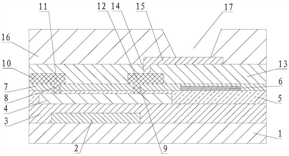
[0055] A TFT array substrate, comprising a substrate 1, a gate formed by a first metal layer 2 disposed on the substrate 1, a gate insulating layer 3 disposed on the substrate 1 and the gate, and a gate insulating layer 3 disposed on the substrate 1. The active layer 4 on the gate insulating layer 3, the etching stopper layer 5 provided on the active layer 4 and the gate insulating layer 3, the auxiliary metal layer 6 provided on the etching stopper layer 5, The passivation layer 7 disposed on the etch barrier layer 5 and the auxiliary metal layer 6 passes through the passivation layer 7 and the etch barrier layer 5 and corresponds to the upper sides of the active layer 4 respectively. The first via hole 8 and the second via hole 9, the third metal layer 10 provided on the passivation layer 7, the third metal layer 10 passes through the first via hole 8 and the second via hole 9 respectively connec...

Embodiment 2

[0060] Please refer to Figure 2 to Figure 4 , the second embodiment of the present invention is:

[0061] A method for preparing a TFT array substrate, comprising the steps of:

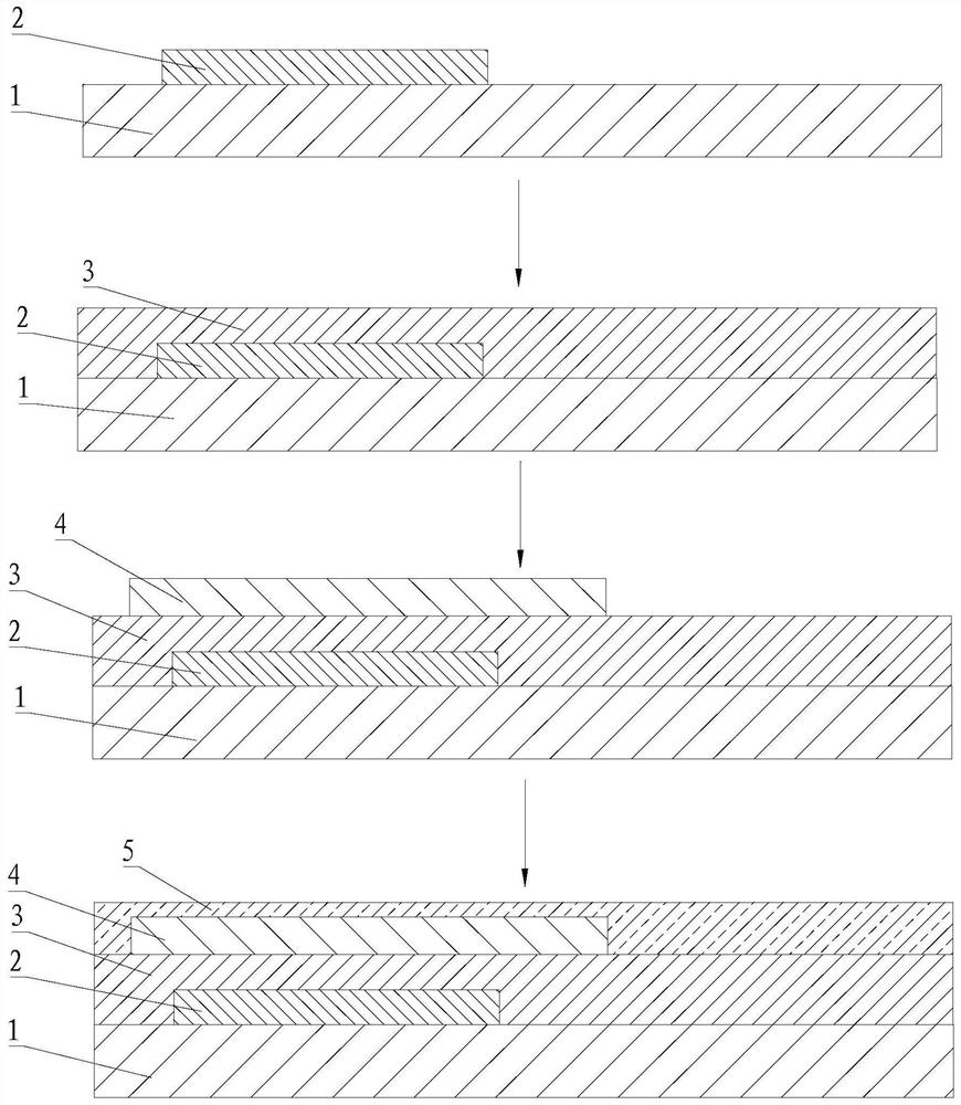
[0062] Step 1: Evaporate the first metal layer (M1) 2 on the substrate 1 by physical vapor deposition (PVD), generally with a Mo / AL / Mo sandwich layer structure, and expose (photo) after photoresist coating, according to the mask Plate (MASK) design to form the required pattern, and then etch the first metal layer (M1) 2 to form the pattern of the gate (GE);

[0063] Step 2: Evaporating a gate insulating layer (GI) 3 on the substrate treated in step 1 by chemical vapor deposition (CVD);

[0064] Step 3: Evaporate an IGZO film on the substrate treated in step 2 by PVD method, and go through exposure (photo), etching (etch) and stripping (stripe) processes; finally form the required active layer (SE)4 picture of;

[0065] Step 4: Evaporating an etching stopper layer (ES) 5 on the substrate treated i...


PUM


Abstract

The invention provides an array substrate structure, a display device and a preparation method of the array substrate structure. A TFT array substrate is provided with a double-layer storage capacitor structure, so the pixel area can be reduced, the PPI of a display panel can be improved, and the flexibility of layout design can be improved on the premise that the capacity of a storage capacitor of a TFT device is guaranteed to be constant and the reliability of the TFT device is guaranteed; besides, the auxiliary metal layer is arranged between the first metal layer and the third metal layer, so that the insulating layers above and below the auxiliary metal layer can be patterned at the same time through a one-time composition process, a mask can be saved, the processes of exposure, etching, stripping and the like of the one-time composition process are reduced, and the process cost of the TFT array substrate is saved. The display device provided by the invention adopts the TFT array substrate, and under the same display size, the pixel distribution density of the display device is greatly improved, and the display picture is clearer.

Description

[0001] This case is a divisional application based on the invention patent with the application date of 2018-03-21, the application number 201810234371.4, and the title "A TFT array substrate, display device, and method for preparing a TFT array substrate". technical field [0002] The invention relates to the field of display technology, in particular to an array substrate structure, a display device and a method for preparing the array substrate structure. Background technique [0003] Since the display screen always has high-definition requirements, this requires the pixel area to be continuously reduced to increase the pixel distribution density (PPI). In recent years, the improvement of the pixel density (PPI) of the display panel is generally limited by the size and wiring pitch of the thin film transistor (TFT) in the pixel structure, and the PPI can be improved by reducing the size of the TFT and the wiring pitch. For example, the method of sharing electrodes is used...

Claims


Application Information

Patent Timeline
Patent Type & Authority Applications(China)
IPC IPC(8): H01L27/12H01L27/32
CPCH01L27/1255H01L27/1259H01L27/1288H10K59/123H10K59/1213H10K59/1216H10K59/131
Inventor 曹尚操
Owner FUJIAN HUAJIACAI CO LTD
Why Eureka
Try Eureka