
Radio frequency microsystem design method and device, electronic equipment and storage medium

A micro-system and radio-frequency technology, applied in computer-aided design, calculation, electrical digital data processing, etc., can solve the problems of lack of atypical radio-frequency system model establishment means, integrated process simulation support, long design cycle, high error probability, etc., to achieve Improve communication efficiency, improve the level of positive design, and improve the effect of design success rate

Inactive Publication Date: 2021-08-13
INFORMATION SCI RES INST OF CETC
View PDF4 Cites 2 Cited by
  • Summary
  • Abstract
  • Description
  • Claims
  • Application Information

AI Technical Summary

Problems solved by technology

[0004] However, the existing RF microsystem design methods usually carry out system design based on a single software, and the sub-modules are generally delivered in the form of models, led by the system designer, and organized by means of telephone and video conferences. Not only lack of atypical System model building methods for radio frequency systems and simulation support for the integration process, and the cost of communication is high, the design cycle is long, and the probability of error is high

Method used


Image

  • Radio frequency microsystem design method and device, electronic equipment and storage medium
  • Radio frequency microsystem design method and device, electronic equipment and storage medium
  • Radio frequency microsystem design method and device, electronic equipment and storage medium

Examples


Embodiment Construction

[0073] In order to enable those skilled in the art to better understand the technical solutions of the present invention, the present invention will be further described in detail below in conjunction with the accompanying drawings and specific embodiments.

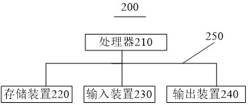
[0074] First, refer to figure 1 An example electronic device for implementing the apparatus and method of the embodiments of the present invention will be described.

[0075] Such as figure 1 As shown, the electronic device 200 includes one or more processors 210, one or more storage devices 220, one or more input devices 230, one or more output devices 240, etc., these components are connected via a bus system 250 and / or other The form of the connecting mechanism interconnects. It should be noted that figure 1 The shown components and structure of the electronic device are exemplary rather than limiting, and the electronic device may also have other components and structures as required.

[0076] The processor 210 ma...


PUM


Abstract

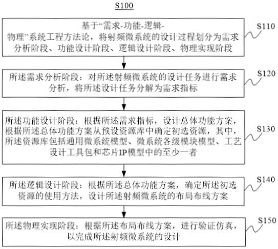
The invention provides a radio frequency microsystem design method and device, electronic equipment and a storage medium. The method comprises the following steps: dividing a design process into a demand analysis stage based on a 'demand-function-logic-physics' system engineering methodology: carrying out demand analysis on a design task, and decomposing the design task into demand indexes; a function design stage: designing an overall function scheme according to the demand indexes, and determining primarily selected resources from a preset resource library according to the overall function scheme; a logic design stage: according to the overall function scheme, determining a use method of the primarily selected resources, and designing a layout and wiring scheme; and a physical implementation stage: performing verification simulation according to the layout and wiring scheme. According to the method, full-process tracking of demand indexes from decomposition refining to simulation verification can be achieved, it is ensured that all design requirements are met, the forward design level is improved, collaborative design based on multiple types of models is achieved, the communication efficiency of different professional engineers is greatly improved, the design period is effectively shortened, and the design success rate is improved.

Description

technical field [0001] The invention belongs to the technical field of microsystem design, and in particular relates to a radio frequency microsystem design method and device, electronic equipment, and a storage medium. Background technique [0002] The microsystem is a new type of microelectronic module with multiple functions and high performance, which is to package and interconnect multiple integrated circuit bare chips at high density on a multi-layer wiring substrate, and then package them together. Microsystems can rationally and effectively integrate digital circuits, analog circuits, microwave circuits, power circuits, and optoelectronic devices to form multi-functional components or systems that cannot be realized by a single professional semiconductor technology, thereby achieving high performance and multi-function of the product change. [0003] A typical radio frequency system demonstration verification prototype mainly includes antennas, transceiver component...

Claims


Application Information

Patent Timeline
IPC IPC(8): G06F30/392
CPCG06F30/392
Inventor 叶雨农王皓岩刘杰
Owner INFORMATION SCI RES INST OF CETC
Learn More