Integrated Micro LED chip and manufacturing method thereof
A manufacturing method and integrated technology, applied to electrical components, electrical solid devices, circuits, etc., can solve problems such as low brightness, low yield, and difficulty in epitaxial growth, so as to save production costs, prevent optical crosstalk, and reduce complexity Effect
- Summary
- Abstract
- Description
- Claims
- Application Information
AI Technical Summary
Problems solved by technology
Method used
Image

Examples
Embodiment 1
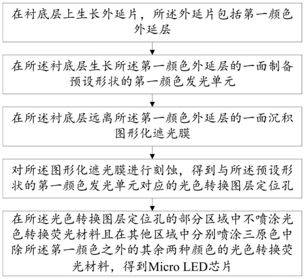
[0067] Please refer to figure 1 , an integrated Micro LED chip manufacturing method, comprising the steps of:
[0068] S1. Growing an epitaxial wafer on the substrate layer, the epitaxial wafer comprising a first color epitaxial layer;
[0069] Wherein, the first color is blue light;
[0070] In an optional embodiment, the substrate layer 1 is a sapphire substrate (Al2O3);
[0071] Specifically, in this embodiment, the thickness of the substrate layer is 650um, and one end of the epitaxial wafer formed from the substrate layer has a gallium nitride buffer layer 2 with a thickness of 2-4um. Blue LED epitaxial wafer, the wavelength of the epitaxial wafer is 400-480nm;
[0072] S2. Prepare a light-emitting unit of the first color with a preset shape on the side of the substrate layer where the epitaxial layer of the first color is grown;
[0073] Wherein, growing the epitaxial layer of the first color on the side of the substrate layer grows a PN junction, a metal oxide curre...
Embodiment 2
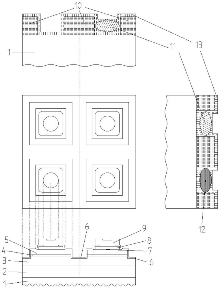
[0100] The difference between this embodiment and Embodiment 1 is that it further defines how to spray the light-color conversion fluorescent material:
[0101] Specifically, there are four positioning holes in the light-color conversion layer arranged in a 2*2 arrangement;
[0102] In the partial area of the positioning hole of the light-color conversion layer, the light-color conversion fluorescent material is not sprayed, and the light-color conversion fluorescent materials of the other two colors except the first color among the three primary colors are sprayed in other areas. Materials include:
[0103] No light color conversion fluorescent material is sprayed in one light color conversion layer positioning hole, red light light color conversion fluorescent material is sprayed in one or two of the light color conversion layer positioning holes, and the remaining number of light color conversion fluorescent materials are sprayed. Spray green light and color conversion f...
Embodiment 3
[0106] Embodiment 3 of the present invention is an integrated Micro LED chip manufacturing method, comprising the following steps:
[0107] Step 1, growing blue light monochromatic GaN epitaxial material, the wavelength range of the epitaxial wafer is 400-475nm, and the substrate is sapphire substrate (Al2O3);
[0108] Step 2. Etching the prepared epitaxial wafer on the front side according to the 2*2 matrix shape, removing part of the P-type gallium nitride, and exposing the lower layer of N-type gallium nitride;
[0109] Step 3, prepare the oxide current spreading layer, what this embodiment uses is indium tin oxide material;
[0110] Step 4, preparing a metal current spreading layer and an etching sacrificial layer, TiPtTi alloy metal is used in this embodiment.
[0111] Step 5, prepare the insulating passivation composite layer, what this embodiment uses is the composite structure of SiO2 and Al2O3, SiO2 is the insulation layer and buffer layer in the lower layer, and Al2...
PUM
| Property | Measurement | Unit |
|---|---|---|
| Thickness | aaaaa | aaaaa |
| Thickness | aaaaa | aaaaa |
| Thickness | aaaaa | aaaaa |
Abstract
Description
Claims
Application Information