

Terahertz material micro-nano defect detection device and method based on multi-frequency point information fusion
A terahertz material and defect detection technology, which is applied in the field of terahertz material micro-nano defect detection devices, can solve the problems of lack of multi-band terahertz signal fusion function, inability to obtain material physical and chemical information, and poor detection accuracy of micro-nano defects. , to improve the far-field detection efficiency of evanescent signals, realize the detection and analysis of micro-nano defects, and facilitate integrated extraction.
- Summary
- Abstract
- Description
- Claims
- Application Information
AI Technical Summary
Problems solved by technology
Method used
Image

Examples
Embodiment 1
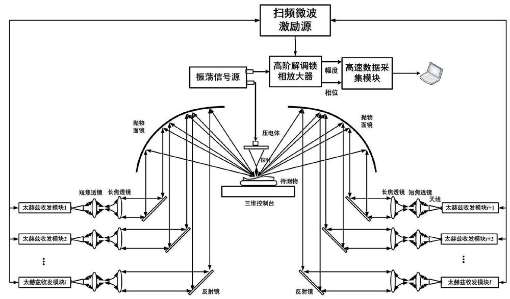
[0076] This embodiment provides a terahertz material micro-nano defect detection device based on multi-frequency point information fusion.
[0077] Micro-nano defect detection device for terahertz materials based on multi-frequency point information fusion, including: microwave excitation source, terahertz transceiver module, mirror combination module, nanoprobe, oscillation signal source, lock-in amplifier and host computer; among them,
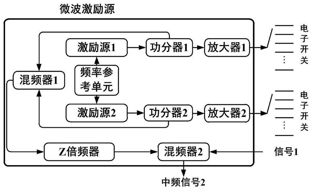
[0078] The microwave excitation source is used to generate the input signal input to the terahertz transceiver module and the mixing signal input to the lock-in amplifier;
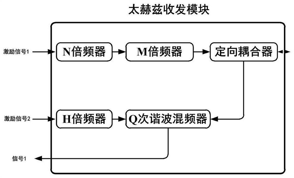
[0079] The terahertz transceiver module is used to continuously radiate terahertz waves and receive evanescent signals that are locally enhanced and modulated by nanoprobes;
[0080] The mirror combination module is used to tightly couple the terahertz beam radiated by the terahertz transceiver module at the tip of the nanoprobe, and reflect the locally enhanced and modu...
Embodiment 2
[0110] This embodiment provides a method for detecting micro-nano defects in terahertz materials based on multi-frequency point information fusion.
[0111] The micro-nano defect detection method of terahertz materials based on multi-frequency point information fusion adopts the above-mentioned micro-nano defect detection device based on multi-frequency point information fusion as described in Embodiment 1, including:
[0112] Control the distance between the sample to be tested and the probe, and make the three-dimensional console move at the nanoscale;
[0113] The terahertz transceiver module continuously radiates terahertz waves and receives the locally enhanced and modulated evanescent signal by the nanoprobe; through phase-locked amplification and high-order demodulation, the amplitude and phase information of the evanescent signal at a certain position of the sample to be tested is obtained;
[0114] The three-dimensional scanning console controls the nanoprobe to trave...
Embodiment 3
[0154] This embodiment provides a method for detecting micro-nano defects in terahertz materials based on multi-frequency point information fusion.
[0155] The micro-nano defect detection method of terahertz materials based on multi-frequency point information fusion adopts the above-mentioned micro-nano defect detection device based on multi-frequency point information fusion as described in Embodiment 1, including:
[0156] Obtain the magnitude matrix and phase matrix of the evanescent signal of the sample to be tested;
[0157] According to the magnitude matrix and phase matrix of the evanescent signal of the sample to be tested, the terahertz near-field imaging algorithm is used to obtain the terahertz near-field image of the sample to be tested at this frequency;
[0158] Obtain the terahertz near-field images of the samples to be tested at all frequencies at specific intervals within the sweep bandwidth, and use the information fusion algorithm based on multiple informa...
PUM
 Abstract
Description
Claims
Application Information