

Film layer removing process for silicon-based OLED micro-display device
A technology for micro-display devices and film layers, which is applied in the manufacturing of electric solid-state devices, semiconductor devices, and semiconductor/solid-state devices, etc., can solve the problems of low film removal efficiency, large number of occupied equipment, abnormal peeling of packaging layers, etc., to avoid Poor etching, reducing process costs, and avoiding abnormal damage to the encapsulation layer
- Summary
- Abstract
- Description
- Claims
- Application Information
AI Technical Summary
Problems solved by technology
Method used
Image


Examples
Embodiment Construction
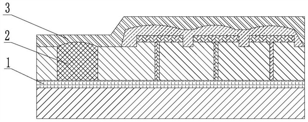
[0028] In order to make the purpose, technical solutions and advantages of the embodiments of the present invention more clear, the technical solutions in the embodiments will be clearly and completely described below in conjunction with the drawings in the embodiments of the present invention. The following embodiments are used to illustrate the present invention , but not to limit the scope of the present invention.
[0029] In the description of the present invention, it should be noted that the terms "upper", "lower", "front", "rear", "left", "right", "vertical", "inner", "outer" etc. The indicated orientation or positional relationship is based on the orientation or positional relationship shown in the drawings, and is only for the convenience of describing the present invention and simplifying the description, rather than indicating or implying that the referred device or element must have a specific orientation, or in a specific orientation. construction and operation, ...
PUM
| Property | Measurement | Unit |
|---|---|---|
| wavelength | aaaaa | aaaaa |
Abstract
Description
Claims
Application Information