Heating device and welding equipment for semiconductor packaging

A heating device and semiconductor technology, applied in semiconductor/solid-state device manufacturing, electrical components, circuits, etc., can solve the problems of inability to meet the heating requirements of 3D-through-silicon via packaging, poor temperature uniformity, and low temperature control accuracy

Pending Publication Date: 2021-09-14
SHENZHEN JT AUTOMATION EQUIP CO LTD
View PDF0 Cites 0 Cited by
  • Summary
  • Abstract
  • Description
  • Claims
  • Application Information

AI Technical Summary

Problems solved by technology

The soldering equipment in the prior art usually uses a hot air reflow heating device to heat the wafer. However, this heating method has low temperature control accuracy and poor temperature uniformity, and is only suitable for traditional SMT (surface mount technology) industry products. welding, but it cannot meet the requirements of relatively high-end welding technology, for example, it cannot meet the heating requirements of 3D-through-silicon via packaging, which has become a short board restricting the development of chip packaging technology

Method used


Image

  • Heating device and welding equipment for semiconductor packaging
  • Heating device and welding equipment for semiconductor packaging
  • Heating device and welding equipment for semiconductor packaging

Examples


Embodiment Construction

[0034] The following will clearly and completely describe the technical solutions in the embodiments of the present invention with reference to the accompanying drawings in the embodiments of the present invention. Obviously, the described embodiments are only some, not all, embodiments of the present invention. Based on the embodiments of the present invention, all other embodiments obtained by persons of ordinary skill in the art without making creative efforts belong to the protection scope of the present invention.

[0035] The core of the present invention is to provide a heating device for semiconductor packaging, which has high temperature control precision and good temperature uniformity. Another core of the present invention is to provide a welding device including the above-mentioned heating device for semiconductor packaging, which has a good welding effect.

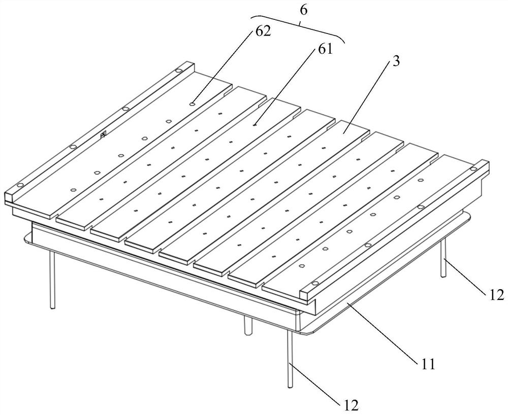
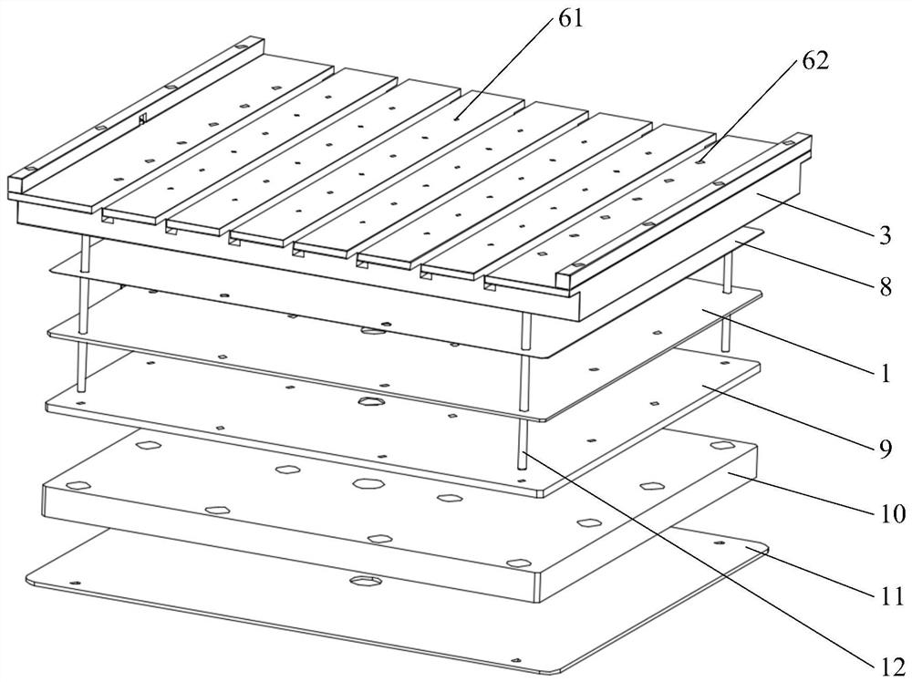
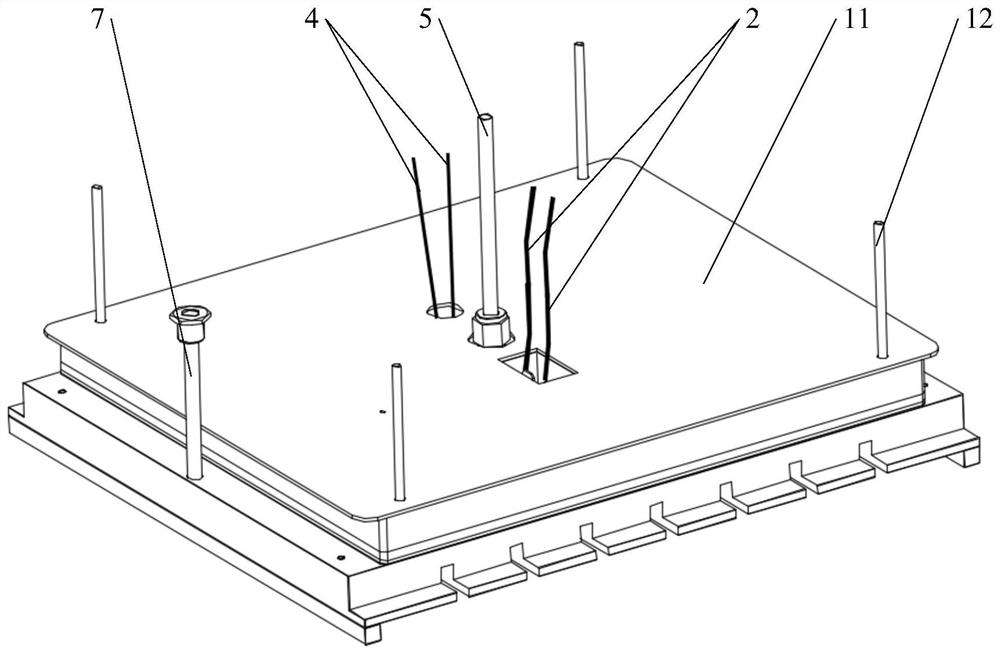
[0036] Please refer to Figure 1-Figure 7 , figure 1 A schematic structural view of a heating device for ...


PUM


Abstract

The invention discloses a heating device and welding equipment for semiconductor packaging, and the device comprises: a heating plate which is used for providing a heat source; a heating plate power line, wherein one end of the heating plate power line is connected with the heating plate, and the other end is connected with an external power supply; and a heating substrate which is connected with the heating plate in an attached mode and used for transferring heat to enable the heat to be uniform, and during heating, a to-be-heated part is placed on the heating substrate. The external power supply is adopted to heat the heating plate, a heat source is provided through the heating plate, and the temperature of the heating plate can be controlled by controlling the heating parameters of the external power supply, so that the temperature of the heating plate is convenient to control, and the temperature control precision can be improved. Besides, the heating substrate is additionally arranged to provide a heating environment for the wafer directly in a contact mode, the heating substrate plays a role in soaking heat, heat of the heating plate can be transferred to the wafer after being uniform, the heating uniformity of the wafer is ensured, and meanwhile the influence of temperature fluctuation of the heating plate on wafer heating can be reduced.

Description

technical field [0001] The invention relates to the technical field of heating process equipment, more specifically, to a heating device for semiconductor packaging. Furthermore, the present invention also relates to a soldering apparatus including the above-mentioned heating device for semiconductor packaging. Background technique [0002] In the field of semiconductor technology, chip manufacturing is inevitably involved. Chip manufacturing mainly includes silicon wafer manufacturing, wafer integrated circuit manufacturing, chip packaging and testing and other links. Among them, chip packaging refers to placing the integrated circuit bare chip on a substrate that acts as a load bearing, then leading out the pins, and then fixing the package as a whole. Chip packaging plays an important role for central processing units and other LSI (Large-scale integrated circuit, large-scale integrated circuits). [0003] With the development of chip packaging technology, the type of c...

Claims


Application Information

Patent Timeline
Patent Type & Authority Applications(China)
IPC IPC(8): H01L21/67
CPCH01L21/6704H01L21/67098H01L21/67121
Inventor 吴限
Owner SHENZHEN JT AUTOMATION EQUIP CO LTD
Why Eureka
Try Eureka