Method for manufacturing semiconductor integrated circuit

A technology for integrated circuits and manufacturing methods, applied in semiconductor/solid-state device manufacturing, semiconductor devices, circuits, etc., can solve the problems of semiconductor integrated circuit operating speed reduction, leakage current reduction, manufacturing difficulties, etc., to improve component separation characteristics, Effect of reducing leakage current and improving operating speed

Inactive Publication Date: 2004-01-07
MITSUBISHI ELECTRIC CORP
View PDF9 Cites 0 Cited by
  • Summary
  • Abstract
  • Description
  • Claims
  • Application Information

AI Technical Summary

Problems solved by technology

Therefore, there is a problem that it is difficult to insert a slit in a wiring narrower than about 0.1 μm in width using the technique described in this publication.
[0026] Conventional isolation trenches of semiconductor integrated circuits are constructed as described above, and there is a problem that microscopic defects are generated on the inner walls of the trenches during etching and heat treatment due to etching damage and contact between materials with different volume expansion rates.
[0027] In addition, in the conventional manufacturing method of semiconductor integrated circuits, when the dielectric constant of the isolation trench is reduced by providing the cavity, there is a problem that the process of providing the cavity in the isolation trench is complicated and the production is difficult.
[0028] In addition, in the conventional semiconductor integrated circuits, there is a problem that the operating speed of the semiconductor integrated circuits is reduced due to the interlayer film provided between the wirings or between the wirings and the semiconductor substrate.
[0029] In the existing manufacturing method of semiconductor devices, the implantation of impurities for forming source / drain regions is performed after forming holes in the sidewall spacers, and the following problems exist in the process: Poor LDD structure with sufficient impurity concentration is difficult
In addition, in order to form a poor LDD structure having a sufficient impurity concentration, the void needs to be made small, so that there is a problem in that since the side wall spacer damaged by ion implantation remains on the source / drain region, the An interface energy level is generated at the interface between the sidewall spacer and the silicon substrate, and a part of the electrons flowing from the source through the drain region to the drain is trapped by the interface energy level, which becomes the main cause of scattering of the leakage current flowing near the interface, reduce leakage current
[0030] In addition, in the conventional semiconductor device and its manufacturing method, there is a problem that the mobility of carriers in the semiconductor substrate directly under the gate insulating film is lowered due to stress applied to the gate electrode, thereby deteriorating the current driving force drop

Method used


Image

  • Method for manufacturing semiconductor integrated circuit
  • Method for manufacturing semiconductor integrated circuit
  • Method for manufacturing semiconductor integrated circuit

Examples


Embodiment 1

[0109] The semiconductor integrated circuit according to Embodiment 1 of the present invention described below includes at least two elements and an isolation trench for isolating the elements, and SiOF which is a fluoride is filled in the isolation trench.

[0110] Here, the case where the effect of the invention is remarkable, that is, the case where the above-mentioned isolation trench is an STI formed on a silicon substrate, will be described.

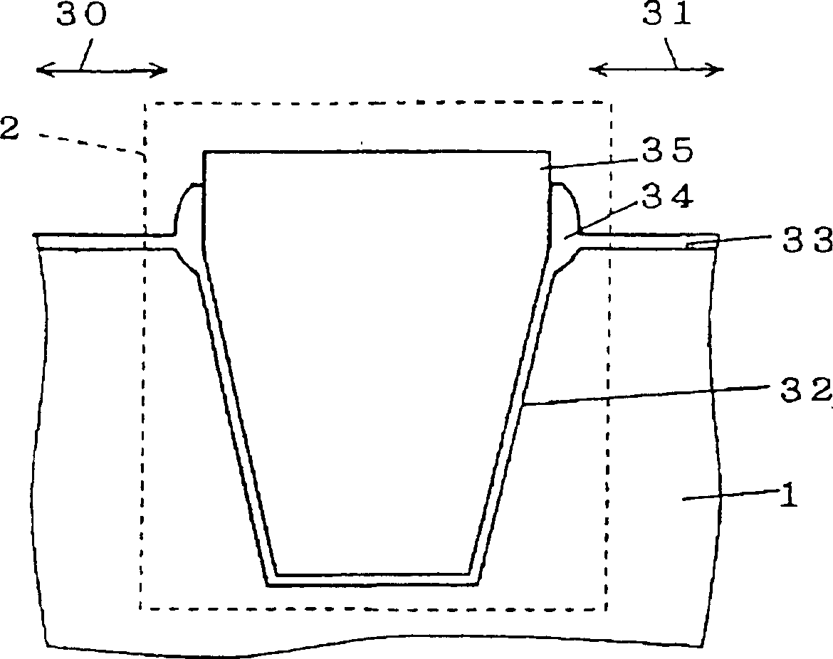
[0111] figure 1 It is a typical diagram showing an example of the structure of the semiconductor integrated circuit of the first embodiment. figure 1 An enlarged cross section of the vicinity of STI2 formed in the semiconductor integrated circuit is shown. In the semiconductor substrate 1, elements separated by STI2 are formed on active semiconductor regions indicated by arrows 30, 31.

[0112] STI2 is formed by silicon oxide film 32 formed on the side wall of the groove, silicon oxide 34 formed in the vicinity of the boundary ...

Embodiment 2

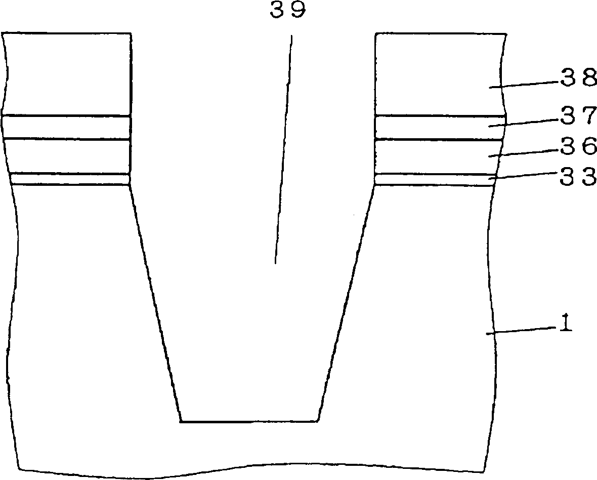
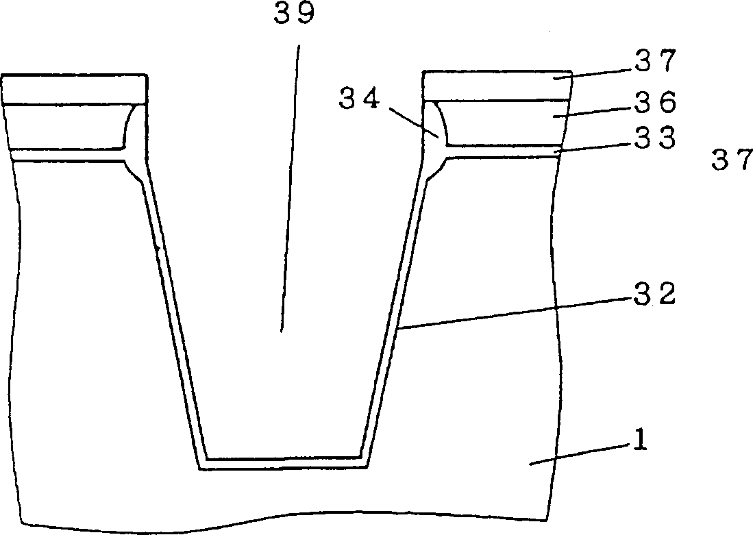
[0121] As described in Example 1, since the relative permittivity of SiOF filled with STI2 is higher than that of SiO 2 Small, so that the element separation characteristics can be improved. A substance with a very small relative permittivity is air, even in Figure 38 with Figure 39 In the conventional separation groove shown in , it is also described in the description of the prior art that the interior is made hollow.

[0122] However, the conventional method of manufacturing the isolation trenches with voids is complicated. The manufacturing method of the semiconductor integrated circuit according to the second embodiment simplifies the step of forming the cavity in the STI.

[0123] Figure 6 ~ Figure 11 It is a typical diagram showing each process of the manufacturing method of the semiconductor integrated circuit of the second embodiment. Figure 6 ~ Figure 11 used in the description of Example 1 Figure 1 to Figure 5 An enlarged cross section of the semiconducto...

Embodiment 3

[0133] The semiconductor integrated circuit of the third embodiment to be described next is characterized in that it forms a cavity under the wiring. Figure 12 It is a layout diagram showing the planar configuration of the semiconductor integrated circuit according to the third embodiment of the present invention. Figure 13 show Figure 12 The cross-section of the B-B line of the semiconductor integrated circuit, Figure 14 show Figure 12 C-C line cross section of a semiconductor integrated circuit.

[0134] exist Figure 12 In this case, a plurality of active semiconductor regions 50 are separated from each other by element isolation regions 51 . The active semiconductor region 50 also constitutes a MOS transistor while constituting the word line 52 laid thereon. will be Figure 12 The bit line 53 arranged perpendicularly to the word line 52 in the plane of , is connected to the source / drain region of the MOS transistor existing in the active semiconductor region 50 ...


PUM


Abstract

Isolation characteristics of an isolation trench can be enhanced. Elements to be isolated by an isolation trench (STI 2) are formed in active semiconductor regions shown by arrows 30 and 31 on a semiconductor substrate 1. The STI 2 is filled with SiOF.

Description

technical field [0001] The present invention relates to a semiconductor integrated circuit, a semiconductor device, a method for manufacturing a semiconductor integrated circuit, and a method for manufacturing a semiconductor device, in particular to element separation used in a semiconductor integrated circuit or a semiconductor device, a sidewall spacer for a MOS transistor, and a method for connecting semiconductor devices. Interlayer insulation of wiring and wiring of integrated circuits. Background technique [0002] Figure 36 with Figure 37 It is a typical diagram showing an example of a conventional semiconductor integrated circuit having an element isolation region. Figure 36 A layout diagram of a semiconductor integrated circuit is shown in . Figure 37 showing along Figure 36 The structure of the profile of the A-A line. [0003] Figure 36 ~ Figure 37 The MOS transistor described in is, for example, a constituent element of a semiconductor memory cell. [...

Claims


Application Information

Patent Timeline
Patent Type & Authority Patents(China)
IPC IPC(8): H01L21/76H01L21/28H01L21/3205H01L21/336H01L21/762H01L21/768H01L21/8242H01L23/522H01L27/108H01L29/423H01L29/49H01L29/78
CPCH01L29/7833H01L29/4983H01L29/42376H01L29/6659H01L21/32053H01L21/28052H01L29/7845H01L29/665H01L21/76235H01L29/42372H01L27/10805H01L29/4933H01L27/10844H01L23/5222H01L23/53295H01L2924/0002H10B12/01H10B12/30H01L2924/00
Inventor 国清辰也
Owner MITSUBISHI ELECTRIC CORP
Why Eureka
Try Eureka