Confinement chemical vapor deposition preparation method of two-dimensional molybdenum ditelluride nano material
A chemical vapor deposition, molybdenum ditelluride technology, applied in binary selenium/tellurium compounds, nanotechnology, metal selenide/telluride, etc., can solve the problem of low experiment repetition rate, poor product stability, and low chemical reaction driving force and other problems, to achieve broad application prospects, stable and controllable process, and good experimental stability.
- Summary
- Abstract
- Description
- Claims
- Application Information
AI Technical Summary
Problems solved by technology
Method used
Image
Examples
Embodiment 1
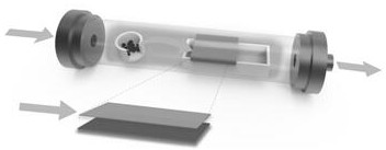
[0045] Preparation of MoTe by Chemical Vapor Deposition 2 method, including the following steps:
[0046] 1) Perform hydrophilic pretreatment on the growth substrate: Cut the silicon substrate with a 280nm thick oxide layer into two silicon wafers with a size of 2cm×1.5cm, and put them in a plasma cleaning machine for surface treatment to make them have Hydrophilicity, set the parameters of the oxygen plasma cleaning machine to the oxygen flow rate of 400sccm, the plasma cleaning power to 40W, and the cleaning time to 50s;
[0047] 2) Introduce sodium molybdate as a molybdenum source: prepare a sodium molybdate solution with a concentration of 0.02 mol / L, put the beaker containing the solution into an ultrasonic instrument, and perform ultrasonication for 5 minutes to make the solution uniform. Put the silicon wafer obtained in step 1 on the spin coater, turn on the vacuum pump to suck it and fix it in the middle of the spin coater, set the spin coater parameters as the first...
Embodiment 2
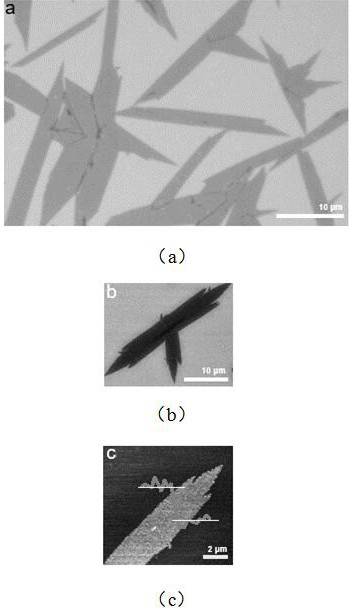
[0052] Embodiment 2: namely the comparative example of the present invention, the operation steps are the same as above, the difference is that the slit spacing of two stacked silicon wafers is set to 520 microns, and its product is as follows Figure 7 As shown, the size of the product is smaller, the nucleation density is lower, and the morphology is close to one-dimensional. Compared with the product in the confined environment (slit spacing of 1-30 μm), it proves that the confined chemical vapor deposition The method is beneficial to the growth of the product, and increases the nucleation density and grain size of the product.
[0053] Examples 2-15 mainly study the preparation of two-dimensional MoTe by chemical vapor deposition 2 During the process, the carrier gas flow rate, confinement slit size, substrate pair synthesis of 2D MoTe 2 The impact of the product, including its size, nucleation density, coverage, thickness, shape, phase, etc. The specific implementation ...
PUM
| Property | Measurement | Unit |
|---|---|---|
| size | aaaaa | aaaaa |
| thickness | aaaaa | aaaaa |
| thickness | aaaaa | aaaaa |
Abstract
Description
Claims
Application Information


