Method for processing semiconductor wafer, semiconductor wafer, clip and semiconductor device

A technology for semiconductors and wafers, applied in the field of semiconductor devices, processing semiconductor wafers, and clamping pads

Pending Publication Date: 2021-09-28
INFINEON TECH AUSTRIA AG
View PDF0 Cites 0 Cited by
  • Summary
  • Abstract
  • Description
  • Claims
  • Application Information

AI Technical Summary

Problems solved by technology

Create defects inside semiconductor wafers

Method used


Image

  • Method for processing semiconductor wafer, semiconductor wafer, clip and semiconductor device
  • Method for processing semiconductor wafer, semiconductor wafer, clip and semiconductor device
  • Method for processing semiconductor wafer, semiconductor wafer, clip and semiconductor device

Examples


example 1

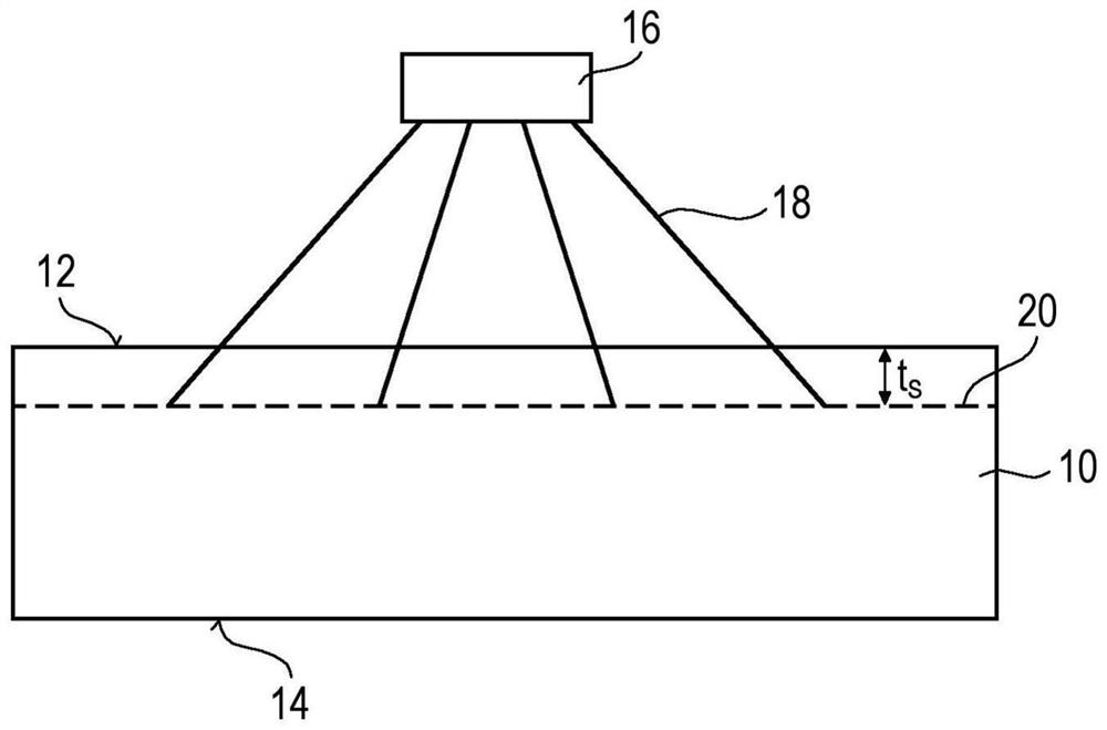
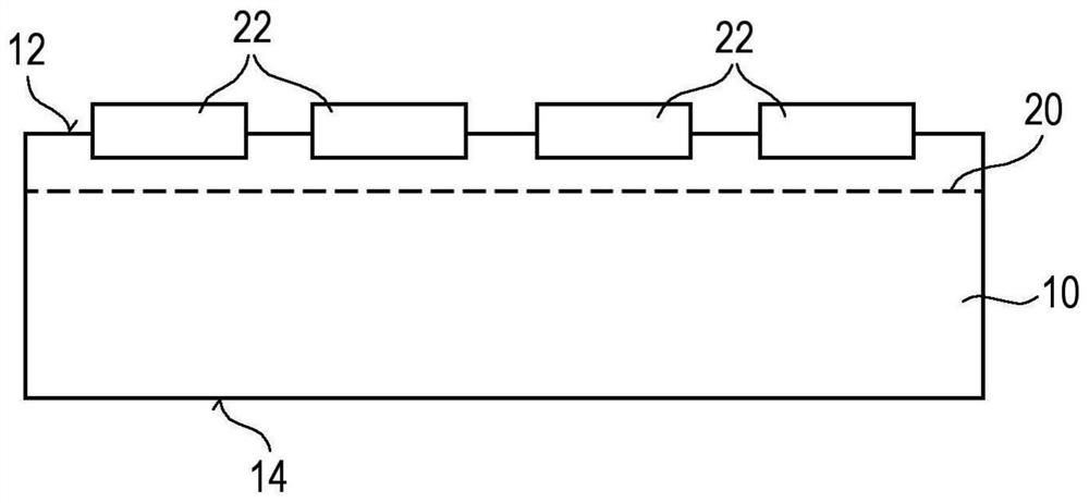
[0060] Example 1 is a method for processing a semiconductor wafer, the method comprising: providing a semiconductor wafer comprising a first main surface and a second main surface opposite to the first main surface; generating a defect inside the semiconductor wafer, the defect defining a breakaway plane parallel to the first major surface; processing the first major surface to define a plurality of electronic semiconductor components; providing a glass structure comprising a plurality of openings; attaching the glass structure to the processed The first major surface, each of the plurality of openings leaving a respective region of the plurality of electronic semiconductor components uncovered; applying a polymer layer to the second major surface; by cooling the polymer layer to its glass transition Below the temperature, the semiconductor wafer is split into semiconductor slices extending between the first main surface and the release surface and comprising a plurality of ele...

example 2

[0061] Example 2 is the method of example 1, wherein the method further comprises applying an additional polymer layer to the first major surface prior to cleaving the semiconductor slices from the semiconductor wafer.

example 3

[0062] Example 3 is the method of Example 1, wherein the thickness of the semiconductor slice is about 100 μm or less, preferably about 50 μm or less.


PUM

PropertyMeasurementUnit
Thicknessaaaaaaaaaa
Thicknessaaaaaaaaaa

Abstract

A method for processing a semiconductor wafer is provided. The semiconductor wafer comprises a first main surface and a second main surface. Defects are generated inside the semiconductor wafer to define a detachment plane parallel to the first main surface. Processing the first main surface defines a plurality of electronic semiconductor components. A glass structure is provided which comprises a plurality of openings. The glass structure is attached to the processed first main surface, each of the plurality of openings leaves a respective area of the plurality of electronic semiconductor components uncovered. A polymer layer is applied to the second main surface, and the semiconductor wafer is split into a semiconductor slice and a remaining semiconductor wafer by cooling the polymer layer beneath its glass transition temperature along the detachment plane. The semiconductor slice comprises the plurality of electronic semiconductor components.

Description

technical field [0001] The present disclosure generally relates to a method for processing semiconductor wafers. The present invention also relates to a semiconductor wafer and a semiconductor device. The present disclosure also relates to a clip for electrically connecting pads arranged on a semiconductor wafer. Background technique [0002] In order to improve the characteristics of a semiconductor device, the final thickness of the semiconductor material in the device is typically reduced. Especially for vertical power devices, the final thickness affects the electrical characteristics. [0003] Semiconductor wafers may be thinned by etching, grinding, sawing, and the like. These removal processes can be time-consuming or resource-intensive. Another method of thinning could be to split the wafer. [0004] The handling of thin wafers is complex. Brittle semiconductor materials break easily once they become thin. Semiconductor wafers to be thinned and already thinned...

Claims


Application Information

Patent Timeline
IPC IPC(8): H01L21/52H01L21/04H01L23/13H01L23/15H01L23/49
CPCH01L21/0445H01L21/52H01L23/13H01L23/15H01L23/49H01L21/7806H01L21/7813H01L2221/6835H01L2221/68377H01L2224/32245H01L2224/04034H01L2224/0224H01L2224/02255H01L2224/0226H01L2224/40105H01L2224/40245H01L2224/40499H01L2224/37147H01L2224/3701H01L2224/40991H01L2224/37013H01L2224/02245H01L24/40H01L24/37H01L24/02H01L2224/73263H01L2224/291H01L2924/014H01L2924/00014H01L24/29H01L24/73H01L24/83H01L24/84H01L24/94H01L2224/29021H01L2224/37012H01L2224/3702H01L2224/73213H01L2224/83851H01L2224/84345
Inventor C·范柯林斯基D·佩多内M·皮钦R·鲁普戴秋莉黄佳艺
Owner INFINEON TECH AUSTRIA AG
Why Eureka
Try Eureka