Sample for measuring doping elements in semiconductor device and preparation method of sample

A technology of doping elements and semiconductors, which is applied in the field of doping element samples and its preparation, can solve the problems of inaccurate measurement and affecting three-dimensional imaging, and achieve the effect of improving accuracy and avoiding damage

Pending Publication Date: 2021-10-08
CHANGXIN MEMORY TECH INC
View PDF6 Cites 0 Cited by
  • Summary
  • Abstract
  • Description
  • Claims
  • Application Information

AI Technical Summary

Problems solved by technology

When performing three-dimensional atom probe measurement, under the same energy, the precipitation rate of silicon atoms in the doped region is greater than that of metal elements, which will affect the final three-dimensional imaging and lead to inaccurate measurements

Method used


Image

  • Sample for measuring doping elements in semiconductor device and preparation method of sample
  • Sample for measuring doping elements in semiconductor device and preparation method of sample
  • Sample for measuring doping elements in semiconductor device and preparation method of sample

Examples


preparation example Construction

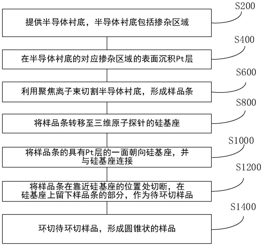
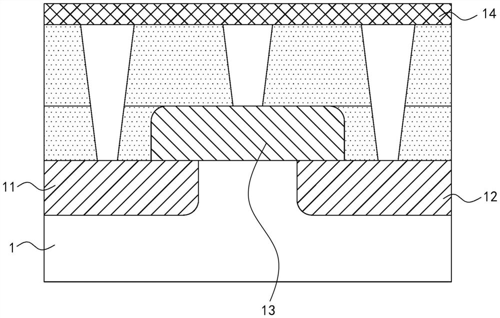
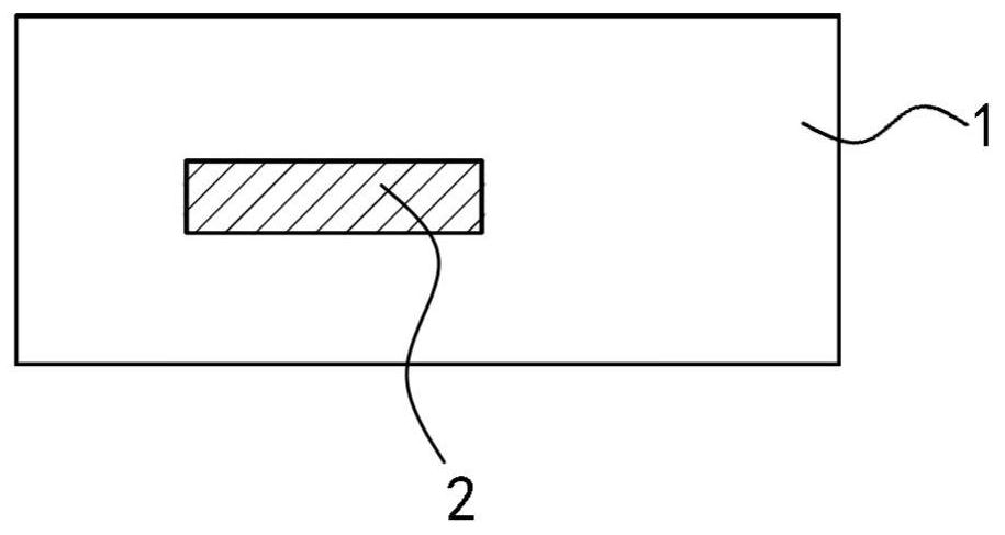
[0042] According to an aspect of the present invention, an embodiment of the present invention provides a method for preparing a sample for measuring dopant elements in a semiconductor device. Such as Figures 1 to 11 As shown, among them, figure 1 shows a flow chart of the preparation method of the present invention, figure 2 A schematic structural view of a semiconductor substrate 1 is shown. Figure 3 to Figure 11 A schematic diagram showing the state of the sample in different steps. Such as figure 1 As shown, the method for preparing a sample for measuring doping elements in a semiconductor device according to an embodiment of the present invention includes:

[0043] Step S200: providing a semiconductor substrate 1 including a doped region.

[0044] Step S400 : depositing a Pt layer 2 on the surface of the corresponding doped region of the semiconductor substrate 1 .

[0045] Step S600 : Cutting the semiconductor substrate 1 with a focused ion beam to form a sample...


PUM

PropertyMeasurementUnit
thicknessaaaaaaaaaa
diameteraaaaaaaaaa
diameteraaaaaaaaaa

Abstract

The invention provides a sample for measuring doping elements in a semiconductor device and a preparation method of the sample. The preparation method comprises the following steps that: a semiconductor substrate is provided, wherein the semiconductor substrate comprises a doped region; a Pt layer is deposited on the surface of the corresponding doped region of the semiconductor substrate; the semiconductor substrate is cut by using a focused ion beam to form a sample strip; the sample strip is transferred to a silicon base of a three-dimensional atom probe; the surface, with the Pt layer, of the sample strip is made to face the silicon base, and connected with the silicon base; the sample strip is cut off at the position close to the silicon base, and the part of the sample strip is left on the silicon base and serves as a sample to be subjected to annular cutting; and the sample to be subjected to annular cutting is subjected to annular cutting to form a conical sample. When the sample prepared by the preparation method disclosed by the invention is subjected to three-dimensional atom probe measurement, the influence of metal elements is avoided, a clearer three-dimensional image can be formed, and the measurement accuracy is improved.

Description

technical field [0001] The invention relates to the technical field of semiconductor manufacturing, in particular to a sample for measuring doping elements in a semiconductor device and a preparation method thereof. Background technique [0002] The 3D atom probe is a measurement and analysis method with atomic-level spatial resolution. When performing three-dimensional atom probe measurement, the sample must be made into a conical shape, so that the sample is connected to a positive high voltage as an anode, and the atoms at the tip of the sample are in a state to be ionized. When a pulse voltage or pulse laser is superimposed on the tip of the sample, the surface atoms will Ionized and evaporated, i.e. the element is precipitated. Time-of-flight mass spectrometry is used to measure the mass-to-charge ratio of evaporated ions to obtain the mass spectrum peak of the ion to determine the element type of evaporated ions. The position-sensitive probe is used to record the two-...

Claims


Application Information

Patent Timeline
Patent Type & Authority Applications(China)
IPC IPC(8): G01N1/28G01Q30/20
CPCG01N1/286G01Q30/20G01N2001/2873
Inventor 王路广
Owner CHANGXIN MEMORY TECH INC
Why Eureka
Try Eureka