Ceramic substrate patterned structure and manufacturing method thereof
A technology of ceramic substrate and manufacturing method, which is applied in semiconductor/solid-state device manufacturing, semiconductor/solid-state device parts, semiconductor devices, etc., can solve problems such as incomplete etching, poor stability, product corrosion, etc., and achieve the copper surface state of the product Good, reduce copper surface roughness, long service life
- Summary
- Abstract
- Description
- Claims
- Application Information
AI Technical Summary
Problems solved by technology
Method used
Image


Examples
Embodiment 1
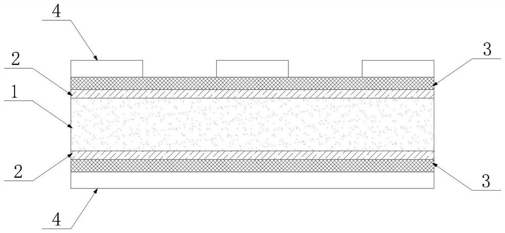
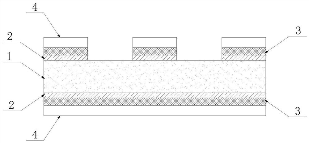
[0042] see Figure 1-4 , the present invention provides the following technical solutions: a ceramic substrate patterned structure, including ceramic substrate 1, bonding layer 2, solder layer 3 and copper platinum 4, bonding layer 2, solder layer 3 and copper platinum layer 4 from inside to outside Attached to the upper and lower surfaces of the ceramic substrate 1 in sequence, the copper-clad ceramic substrate manufactured by the active brazing method of the ceramic substrate 1, the bonding layer 2, the solder layer 3 and the copper platinum 4 is exposed and developed by etching The copper-clad ceramic substrate is etched by the liquid to form a patterned structure of the ceramic substrate. The ceramic substrate 1 is a nitride ceramic or an oxide ceramic. The solder layer 3 is composed of Ag, Cu and Ti components, and the Ag content is more than 70%. , the rest are Cu and Ti, the etchant contains hydrogen peroxide, ammonia water, the structure contains carboxyl groups and th...
PUM
 Abstract
Description
Claims
Application Information
 - R&D
- Intellectual Property
- Life Sciences
- Materials
- Tech Scout
- Unparalleled Data Quality
- Higher Quality Content
- 60% Fewer Hallucinations
Browse by: Latest US Patents, China's latest patents, Technical Efficacy Thesaurus, Application Domain, Technology Topic, Popular Technical Reports.
© 2025 PatSnap. All rights reserved.Legal|Privacy policy|Modern Slavery Act Transparency Statement|Sitemap|About US| Contact US: help@patsnap.com