Over-discharge prevention negative electrode, preparation method thereof and battery
An over-discharge and negative electrode technology, applied in the direction of negative electrodes, battery electrodes, secondary batteries, etc., can solve the problems of carbon negative electrode capacity exhaustion, negative electrode current collector copper dissolution, potential rise, etc. The process is simple and the effect of preventing over-discharge
- Summary
- Abstract
- Description
- Claims
- Application Information
AI Technical Summary
Problems solved by technology
Method used
Image

Examples
preparation example Construction
[0045] In another specific embodiment, the present invention provides a method for preparing the above-mentioned anti-overdischarge negative electrode, the preparation method comprising:
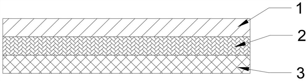
[0046] At least one side surface of the current collector 3 is coated with an anti-overdischarge functional layer 2 including a niobium-titanium compound, and a negative electrode active material layer 1 is prepared by coating the surface of the anti-overdischarge functional layer 2 .
Embodiment 1
[0048] This embodiment provides an anti-over-discharge negative electrode. One side surface of the current collector 3 is sequentially provided with an anti-over-discharge functional layer 2 and a negative electrode active material layer 1. The anti-over-discharge functional layer 2 includes a first binder and TiNb 2 o 7 . TiNb in anti-over-discharge layer 2 2 o 7 The mass content is 75%. The thickness of the anti-over-discharge functional layer 2 is 5 μm, and the first binder is polyimide.
[0049] The negative electrode active material layer 1 includes a negative electrode active material, a conductive agent and a second binder in a mass ratio of 97:1:2. The negative electrode active material is graphite; the conductive agent is super P; the second binder is polyimide.
Embodiment 2
[0051] This embodiment provides an anti-over-discharge negative electrode. The surfaces of both sides of the current collector 3 are sequentially stacked with an anti-over-discharge functional layer 2 and a negative electrode active material layer 1. The anti-over-discharge functional layer 2 includes a first binder and TiNb 2 o 7 . TiNb in anti-over-discharge layer 2 2 o 7 The mass content is 50%. The thickness of the anti-over-discharge functional layer 2 is 10 μm.
[0052] The negative electrode active material layer 1 is exactly the same as that in Example 1.
PUM
| Property | Measurement | Unit |
|---|---|---|
| Thickness | aaaaa | aaaaa |
| Thickness | aaaaa | aaaaa |
| Thickness | aaaaa | aaaaa |
Abstract
Description
Claims
Application Information
 - R&D
- Intellectual Property
- Life Sciences
- Materials
- Tech Scout
- Unparalleled Data Quality
- Higher Quality Content
- 60% Fewer Hallucinations
Browse by: Latest US Patents, China's latest patents, Technical Efficacy Thesaurus, Application Domain, Technology Topic, Popular Technical Reports.
© 2025 PatSnap. All rights reserved.Legal|Privacy policy|Modern Slavery Act Transparency Statement|Sitemap|About US| Contact US: help@patsnap.com