OLED device and preparation method
A technology of devices and organic light-emitting elements, which is applied in the field of OLED displays, can solve problems such as performance waste, achieve the effects of reducing production costs, simplifying device structure design, and reducing sub-pixel spacing
- Summary
- Abstract
- Description
- Claims
- Application Information
AI Technical Summary
Problems solved by technology
Method used
Image
Examples
Embodiment Construction
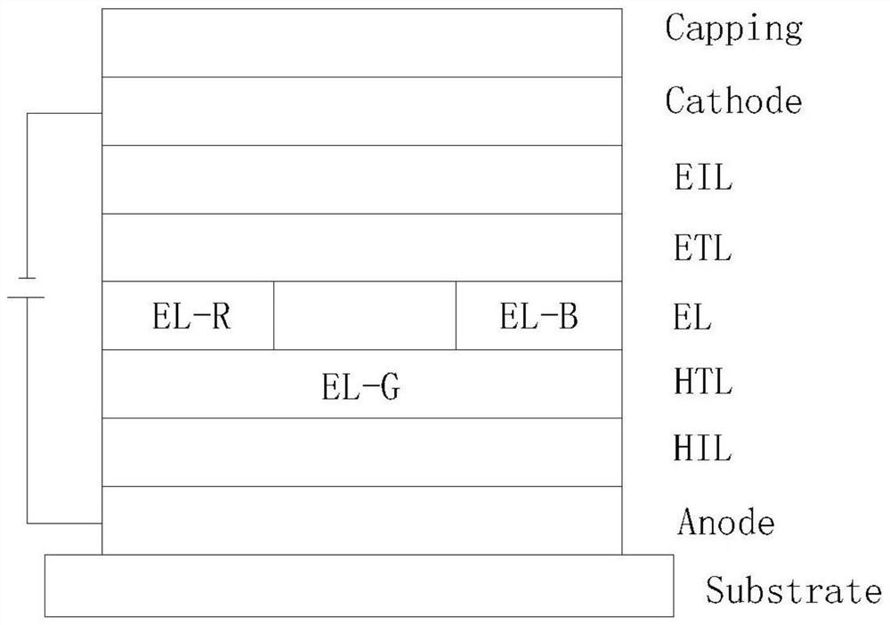
[0020] see figure 1 , In an embodiment, an OLED device includes a substrate Substrate and an anode Anode, a hole injection layer HIL, a hole transport layer HTL, a light emitting layer EL, an electron transport layer ETL, an electron injection layer EIL, and a cathode are sequentially arranged on the substrate Substrate Cathode and sealing film layer Capping, the light-emitting layer EL includes a red light region EL-R, a blue light region EL-B and a green light region EL-G, and the red light region EL-R is provided with a red light organic light-emitting element; The blue light region EL-B of the light-emitting layer is provided with a blue light organic light-emitting element, and the green light region EL-G is excited and formed by the material of the hole transport layer.
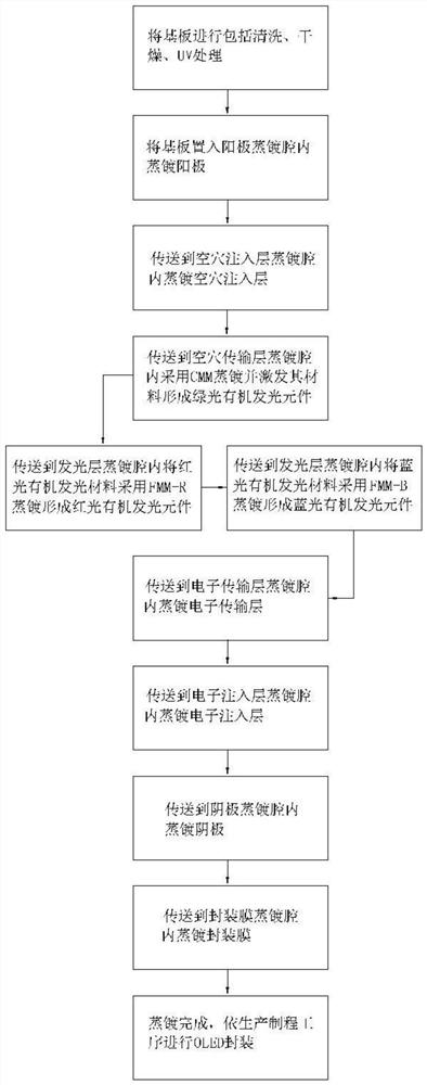
[0021] see figure 2 , the preparation method of the above-mentioned OLED device, the substrate is subjected to cleaning, drying, and UV treatment before evaporation, and then the substrate is transfer...
PUM
 Abstract
Description
Claims
Application Information
 - R&D Engineer
- R&D Manager
- IP Professional
- Industry Leading Data Capabilities
- Powerful AI technology
- Patent DNA Extraction
Browse by: Latest US Patents, China's latest patents, Technical Efficacy Thesaurus, Application Domain, Technology Topic, Popular Technical Reports.
© 2024 PatSnap. All rights reserved.Legal|Privacy policy|Modern Slavery Act Transparency Statement|Sitemap|About US| Contact US: help@patsnap.com


