Reusable optical biosensor chip and method for realizing reuse of optical biosensor chip
A biosensor and biosensing technology, applied in the field of biosensing, can solve the problems of unsatisfactory reuse effect, irremovable, cumbersome steps, etc., and achieve the effect of reuse
- Summary
- Abstract
- Description
- Claims
- Application Information
AI Technical Summary
Problems solved by technology
Method used
Image
Examples
Embodiment 1
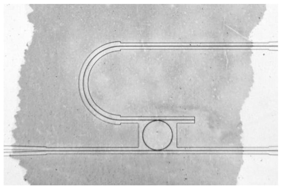
[0045] The optical biosensor chip used in this embodiment is a waveguide microring sensor chip (core structure such as figure 2 As shown), the microring is prepared by using the 180nm silicon photonics product line of the Institute of Microelectronics, on the SOI substrate, through electron beam lithography EBL and reactive ion etching RIE process. The micro-ring chip is composed of an optical coupler, a micro-ring, a through-end and a download end. The radius of the micro-ring is 20 μm, the gap between the micro-ring and the through-end is 250 nm, the height of the ridge waveguide is 70 nm, and the width is 450 nm.
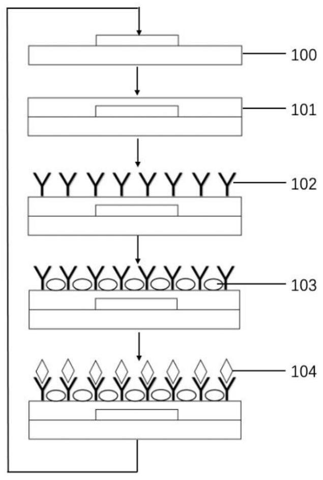
[0046] A method to achieve the reuse of optical biosensing chips:
[0047] (1) Soak the above-mentioned waveguide microring sensor chip in a hydrofluoric acid solution, remove the surface silicon dioxide layer, and expose the waveguide surface;
[0048] (2) Place the chip exposed on the surface of the waveguide in acetone, ethanol and deionized water in sequenc...
PUM
| Property | Measurement | Unit |
|---|---|---|
| Length | aaaaa | aaaaa |
| Thickness | aaaaa | aaaaa |
Abstract
Description
Claims
Application Information


