Regulation and control method of quantum well and quantum dot material energy band structure
A technology of quantum dot material and energy band structure, applied in nanotechnology for materials and surface science, sustainable manufacturing/processing, electrical components, etc., can solve problems such as high cost and low production efficiency, and improve production efficiency , cost reduction, and significant application prospects
- Summary
- Abstract
- Description
- Claims
- Application Information
AI Technical Summary
Problems solved by technology
Method used
Image
Examples
Embodiment 1
[0041]A method for regulating the energy band structure of a quantum well and a quantum dot material in this embodiment comprises the following steps:
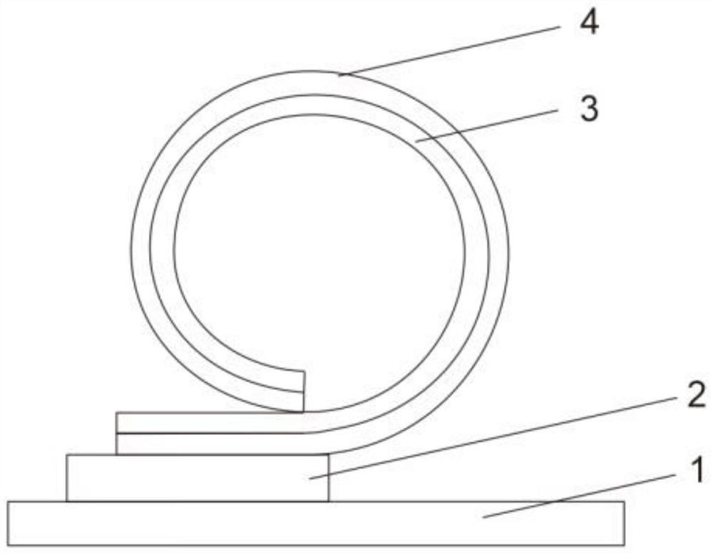
[0042] Step 1, using molecular beam epitaxy to grow the sacrificial layer AlAs (30nm) and the stress-introducing layer In in sequence on the GaAs substrate 0.2 al 0.2 Ga 0.6 As(20nm) and quantum well material GaAs(6.5nm) / Al 0.26 Ga 0.74 Quantum structure thin film functional layer composed of As (30nm).
[0043] Step 2: Etching the rectangular opening area of the sacrificial layer by photolithography, using citric acid, hydrogen peroxide mixed solution (6:1) and hydrofluoric acid (10%) to etch alternately to etch the stress introducing layer and the functional layer of the quantum structure film to the sacrificial layer.
[0044] The hydrogen peroxide mixed solution is obtained by mixing citric acid solution obtained from citric acid powder and water at a ratio of 1:1 and 30% hydrogen peroxide at a ratio of 6:1.
[004...
Embodiment 2
[0054] A method for regulating the energy band structure of a quantum well and a quantum dot material in this embodiment comprises the following steps:
[0055] Step 1, grow the buffer layer n sequentially on the Si substrate using molecular beam epitaxy + GaAs (10nm), sacrificial layer AlAs (20nm), stress layer In 0.2 al 0.2 Ga 0.6 As(20nm) and quantum well material GaAs(6.5nm) / Al 0.26 Ga 0.74 Quantum structure thin film functional layer composed of As (30nm).
[0056] Step 2: Etching the rectangular opening area of the sacrificial layer by photolithography, using citric acid, hydrogen peroxide mixed solution (6:1) and hydrofluoric acid (10%) to etch alternately to etch the stress introducing layer and the functional layer of the quantum structure film to the sacrificial layer.
[0057] Step 3, use hydrofluoric acid (5%) to corrode part of the sacrificial layer through the rectangular opening area, release the stress introduction layer and the quantum structure thin f...
Embodiment 3
[0060] A method for regulating the energy band structure of a quantum well and a quantum dot material in this embodiment comprises the following steps:
[0061] Step 1, using molecular beam epitaxy to grow the sacrificial layer AlAs (30nm) and the stress layer In in sequence on the Si substrate 0.2 al 0.2 Ga 0.6 Quantum structure thin film functional layer composed of As (10nm) and quantum dot material InP.
[0062] Step 2: Etching the rectangular opening area of the sacrificial layer by photolithography, using citric acid, hydrogen peroxide mixed solution (6:1) and hydrofluoric acid (10%) to etch alternately to etch the stress introducing layer and the functional layer of the quantum structure film to the sacrificial layer.
[0063] Step 3, use hydrofluoric acid (5%) to corrode part of the sacrificial layer through the rectangular opening area, release the stress introduction layer and the quantum structure thin film functional layer, and after prestress release, the str...
PUM
 Abstract
Description
Claims
Application Information
 - R&D
- Intellectual Property
- Life Sciences
- Materials
- Tech Scout
- Unparalleled Data Quality
- Higher Quality Content
- 60% Fewer Hallucinations
Browse by: Latest US Patents, China's latest patents, Technical Efficacy Thesaurus, Application Domain, Technology Topic, Popular Technical Reports.
© 2025 PatSnap. All rights reserved.Legal|Privacy policy|Modern Slavery Act Transparency Statement|Sitemap|About US| Contact US: help@patsnap.com


