LNOI-based spot-size converter directly coupled with single-mode fiber
A single-mode fiber and converter technology, applied in the field of integrated optics, can solve the problems of difficulty in achieving high coupling bandwidth and polarization independence, lack of encapsulation solutions for grating coupling, limited alignment tolerance, etc., which is conducive to large-scale optical circuit integration, The overall structure is compact and the coupling efficiency is improved
- Summary
- Abstract
- Description
- Claims
- Application Information
AI Technical Summary
Problems solved by technology
Method used
Image

Examples
Embodiment Construction
[0021] An embodiment of the present invention will be further described below in conjunction with the accompanying drawings, but the present invention is not limited to this embodiment, and within the spirit and principles of the present invention, any modifications, equivalent replacements, improvements, etc. within the scope of protection of the invention.
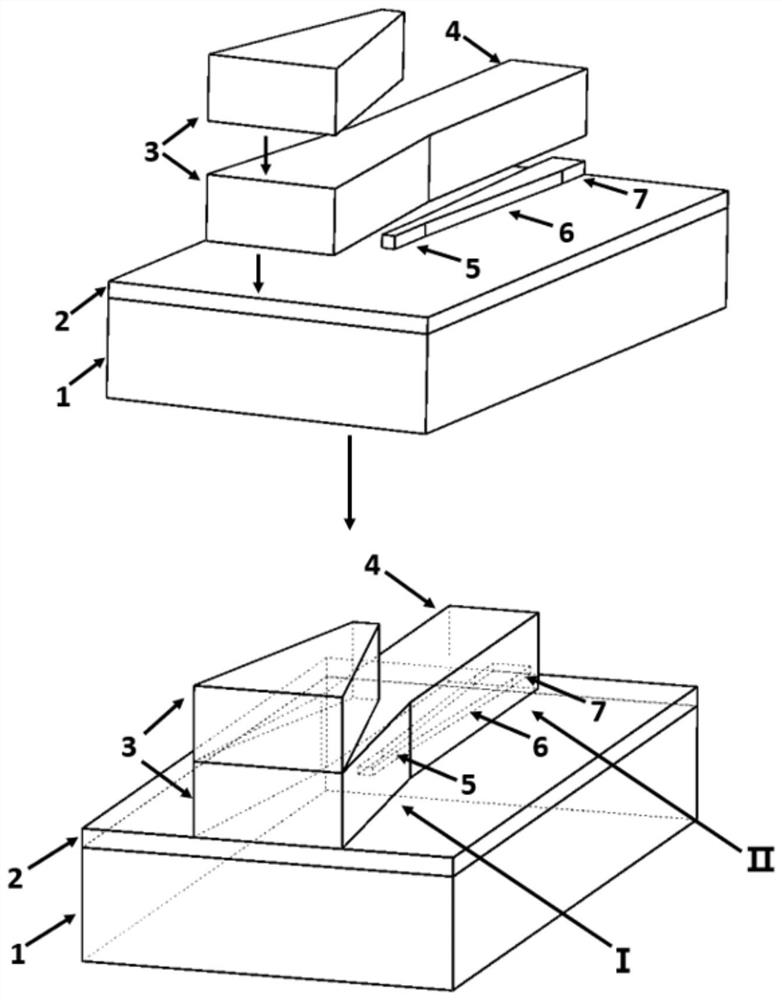
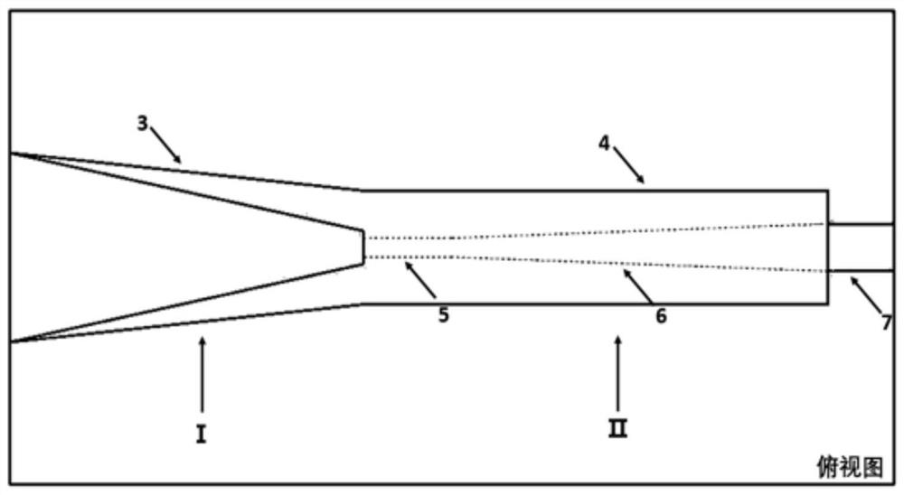
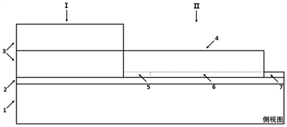
[0022] A schematic diagram of an LNOI fundamental mode spot converter directly coupled with a single-mode fiber in this embodiment is shown in FIG. 1 .
[0023] This embodiment is used for coupling between the single-mode fiber and the LNOI chip, the left end face of the double-layer forward tapered waveguide (3) in the double-layer forward tapered region (I) is docked with the single-mode fiber, and the reverse tapered region ( In II), the output lithium niobate waveguide (7) is docked with the LNOI chip waveguide to realize the mode field conversion between the large mode field of the single-mode fiber and the small mo...
PUM
| Property | Measurement | Unit |
|---|---|---|
| Thickness | aaaaa | aaaaa |
| Thickness | aaaaa | aaaaa |
| Thickness | aaaaa | aaaaa |
Abstract
Description
Claims
Application Information
 - R&D
- Intellectual Property
- Life Sciences
- Materials
- Tech Scout
- Unparalleled Data Quality
- Higher Quality Content
- 60% Fewer Hallucinations
Browse by: Latest US Patents, China's latest patents, Technical Efficacy Thesaurus, Application Domain, Technology Topic, Popular Technical Reports.
© 2025 PatSnap. All rights reserved.Legal|Privacy policy|Modern Slavery Act Transparency Statement|Sitemap|About US| Contact US: help@patsnap.com