Eureka AIR delivers breakthrough ideas for toughest innovation challenges, trusted by R&D personnel around the world.

Ultrahigh-frequency and ultra-wide-band composite electromagnetic wave-absorbing structure

A composite electromagnetic and ultra-broadband technology, applied in electrical components, antennas, etc., can solve the problems of difficult to meet impedance matching conditions and large relative permittivity.

Pending Publication Date: 2021-11-16
海宁利伊电子科技有限公司
View PDF5 Cites 0 Cited by
  • Summary
  • Abstract
  • Description
  • Claims
  • Application Information

AI Technical Summary

Problems solved by technology

However, most commercial absorbing materials can only meet the attenuation loss conditions, but it is difficult to meet the impedance matching conditions. This is due to the limitations of processes, materials and other factors, which make their relative permittivity relatively large.

Method used


Image

  • Ultrahigh-frequency and ultra-wide-band composite electromagnetic wave-absorbing structure
  • Ultrahigh-frequency and ultra-wide-band composite electromagnetic wave-absorbing structure
  • Ultrahigh-frequency and ultra-wide-band composite electromagnetic wave-absorbing structure

Examples


example

[0034] Example: Radiation suppression in a chip package scenario with a heat sink loaded:

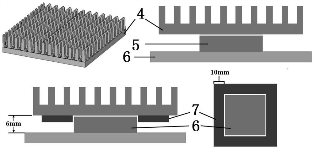
[0035] image 3It is a schematic diagram of a packaging scene of a chip 6 loaded with a metal heat sink 5, and a schematic diagram of an arrangement method of a wave-absorbing structure (or wave-absorbing material) in this packaging scene. Among them, the electromagnetic radiation from the integrated circuit in the chip 5 will leak out through the gap between the heat sink 4 and the printed circuit board 6 , causing a serious problem of excessive EMI radiation. The method to solve this problem is to paste the composite electromagnetic wave-absorbing material 7 under the radiator 4 to absorb electromagnetic radiation. In this example, the composite electromagnetic wave-absorbing material 7 is all pasted on the bottom of the radiator 4 and around the chip 5 in a "back shape", the distance between the radiator 4 and the printed circuit board 6 is 6mm, and the wave-absorbing structure (wav...


PUM

PropertyMeasurementUnit
thicknessaaaaaaaaaa
thicknessaaaaaaaaaa
thicknessaaaaaaaaaa

Abstract

The invention provides an ultrahigh-frequency and ultra-wide-band composite electromagnetic wave-absorbing structure. The wave-absorbing material can achieve the radiation suppression effect of 10 dB or above at 20-30 GHz, and the wave-absorbing effect is obviously improved compared with the wave-absorbing effect obtained by independently using a commercial wave-absorbing material. The ultrahigh-frequency and ultra-wide-band composite electromagnetic wave-absorbing structure comprises a plurality of wave absorbing units which are arranged periodically; each wave absorbing unit comprises a top layer, a middle layer and a bottom layer which are sequentially arranged from top to bottom, the bottom layer is a metal back plate, the middle layer is a commercial electromagnetic wave-absorbing material, and the top layer is a Rogers RO4725JXR material.

Description

technical field [0001] The invention relates to the field of electromagnetic wave-absorbing materials, in particular to a composite electromagnetic wave-absorbing structure of ultra-high frequency and ultra-wideband. Background technique [0002] The chip is the "brain" of the current communication system, and the integrated circuit in the chip is usually the main source of electromagnetic compatibility (EMC) problems. On the one hand, its complex electromagnetic stray signals will interfere with other surrounding functional modules. Its strong radiation will even cause EMC problems of the whole system, seriously restricting the performance improvement of the equipment and even causing the paralysis of the equipment. With the increase of the operating frequency of electronic devices, the problem of electromagnetic radiation in the high frequency band (above 20 GHz) becomes more and more difficult to solve. It leaks from the gap between the device and the printed circuit boa...

Claims


Application Information

Patent Timeline
Patent Type & Authority Applications(China)
IPC IPC(8): H01Q17/00
CPCH01Q17/00
Inventor 李尔平梁星磊邢家琦
Owner 海宁利伊电子科技有限公司
Why Eureka
Eureka Blog
Learn More