Linear polarization narrow linewidth external cavity type semiconductor laser

A linearly polarized, narrow linewidth technology, applied to the field of linearly polarized narrow linewidth external cavity semiconductor lasers

Active Publication Date: 2021-11-16
CHANGCHUN INST OF OPTICS FINE MECHANICS & PHYSICS CHINESE ACAD OF SCI
View PDF3 Cites 0 Cited by
  • Summary
  • Abstract
  • Description
  • Claims
  • Application Information

AI Technical Summary

Problems solved by technology

[0005] The object of the present invention is to propose a linearly polarized narrow linewidth external cavity semiconductor laser to overcome the linearly polarized narrow lin

Method used


Image

  • Linear polarization narrow linewidth external cavity type semiconductor laser
  • Linear polarization narrow linewidth external cavity type semiconductor laser
  • Linear polarization narrow linewidth external cavity type semiconductor laser

Examples


Embodiment 1

[0062] The linearly polarized narrow-linewidth external-cavity semiconductor laser provided in Embodiment 1 of the present invention includes a gain chip 101, an external-cavity frequency selection device 102, a coupling lens 103, a lens group 104, an L-shaped bracket 105, a polarization-maintaining fiber 106, and a metal bracket 107 and a substrate 108, the substrate 108 is a metal substrate, the gain chip 101, the external cavity frequency selection device 102, the coupling lens 103, the lens group 104, the L-shaped bracket 105, the polarization maintaining optical fiber 106, and the metal bracket 107 are respectively arranged on the substrate Bottom 108 on.

[0063] The F-P resonant cavity is formed between the gain chip 101 and the frequency selection device 102 of the external cavity, and the coupling lens 103 is located between the gain chip 101 and the frequency selection device 102 of the external cavity, and is used to match the mode field of the gain chip and the freq...

Embodiment 2

[0073] The difference between Embodiment 2 and Embodiment 1 is that the coupling mode between the gain chip 201 and the external cavity frequency selection device 202 is changed from lens coupling to end surface coupling. More specifically, the positions of the gain chip 201 and the external cavity frequency selection device 202 are exchanged with those of the gain chip 101 and the external cavity frequency selection device 102 in Embodiment 1, and the gain chip 201 is used as a linearly polarized narrow linewidth external cavity type At the output end of the semiconductor laser, the external cavity frequency selection device 202 is used as the high inversion end of the linearly polarized narrow linewidth external cavity type semiconductor laser, and the gain chip 201 and the external cavity frequency selection device 202 are directly integrated through end-face coupling.

[0074] An anti-reflection film is plated on the end face of the gain chip 201 coupled with the external c...

Embodiment 3

[0077] The difference between Embodiment 3 and Embodiment 1 is that the coupling lens 103 in Embodiment 1 is replaced by a speckle converter 303, and the speckle converter 303 is integrated at the front end of the external cavity frequency selection device 302, and the structure of the speckle converter 303 It is an inverted cone, in the same layer as the waveguide, and has the same thickness as the waveguide. The function of the mode speckle converter 303 is the same as that of the coupling lens 103 in Embodiment 1, and is used to match the mode field between the gain chip 301 and the external cavity frequency selection device 302, and improve the gain chip 301 and the external cavity frequency selection device 302. Coupling efficiency between.

[0078] The structures and positions of the lens group 304, the L-shaped bracket 305, the polarization-maintaining fiber 306, the metal bracket 307, and the substrate 308 in Embodiment 3 are all the same as those of the lens group 104...


PUM


Abstract

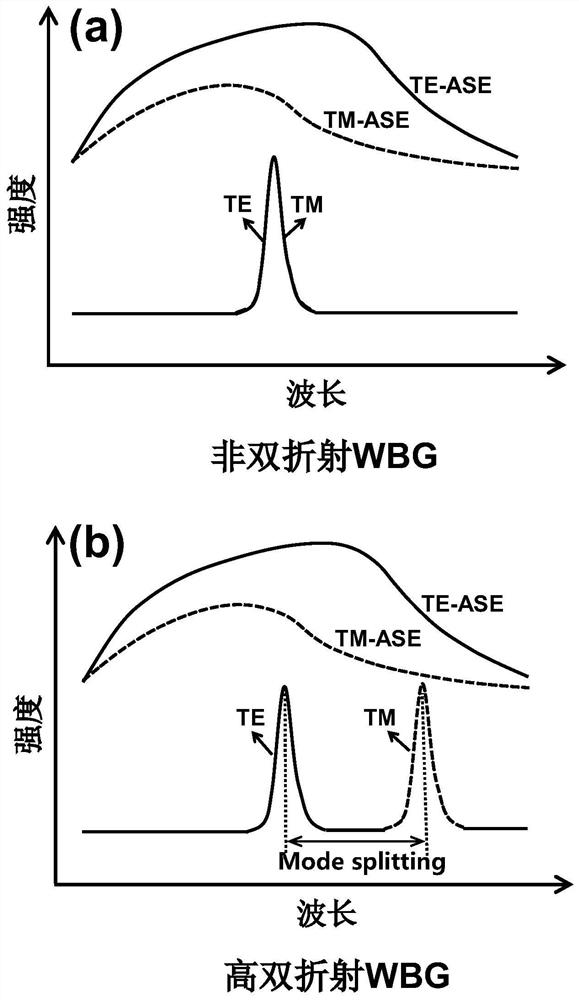
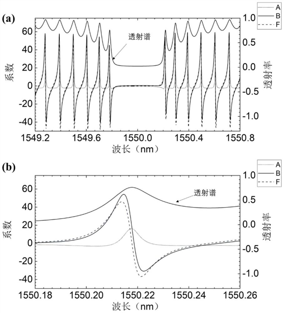
The invention provides a linear polarization narrow linewidth external cavity type semiconductor laser, which comprises a gain chip and an external cavity frequency selection device. The basic structure of the external cavity frequency selection device is a silicon-based waveguide Bragg grating, and based on the birefringence effect of the silicon-based waveguide Bragg grating, the TE mode and the TM mode reflected by the external cavity frequency selection device are split. And when the TE mode and the TM mode are reflected back to the gain chip and injected to the ASE spectrum of the gain chip, a gain difference is formed between the TE mode and the TM mode, and the gains of the TM mode and the TM mode are inhibited, so that the linear polarization narrow linewidth external cavity type semiconductor laser outputs in a linear polarization mode. Linear polarization laser can be output without a polarization controller, so that the structure of the external cavity semiconductor laser is simplified, and loss among components in the external cavity semiconductor laser is reduced.

Description

technical field [0001] The invention relates to the technical field of optoelectronic devices, in particular to a linearly polarized narrow-linewidth external-cavity semiconductor laser. Background technique [0002] Narrow linewidth semiconductor lasers have the characteristics of narrow spectral linewidth, good coherence performance, low phase frequency noise and low relative intensity noise (RIN). There are a wide range of applications in fields such as lasers, and the linewidth level of the laser is generally required to reach the kHz level. The currently commonly used narrow-linewidth semiconductor lasers usually use monolithic integrated Distributed Bragg reflector (DBR) lasers and distributed Bragg feedback (Distributed Bragg feedback, DFB) lasers. The cavity lengths of these two lasers are usually short, which determines The photon lifetime is short, which limits the linewidth performance. The linewidth of these two lasers is generally at the MHz level, which is dif...

Claims


Application Information

Patent Timeline
IPC IPC(8): H01S5/068H01S5/14
CPCH01S5/141H01S5/068
Inventor 陈超罗曦晨宁永强张星秦莉王立军
Owner CHANGCHUN INST OF OPTICS FINE MECHANICS & PHYSICS CHINESE ACAD OF SCI
Why Eureka
Try Eureka