

Self-aligned graphene field emission gate structure and preparation method thereof
A technology of self-alignment and emission grid, which is applied in cold cathode manufacturing, electrode system manufacturing, discharge tube/lamp manufacturing, etc., can solve the problems of controllable etching of graphene layer, high current density, and electron transmittance. Low-level problems, to achieve the effect of improving electron transmittance and reducing modulation voltage
- Summary
- Abstract
- Description
- Claims
- Application Information
AI Technical Summary
Problems solved by technology
Method used
Image

Examples
Embodiment Construction
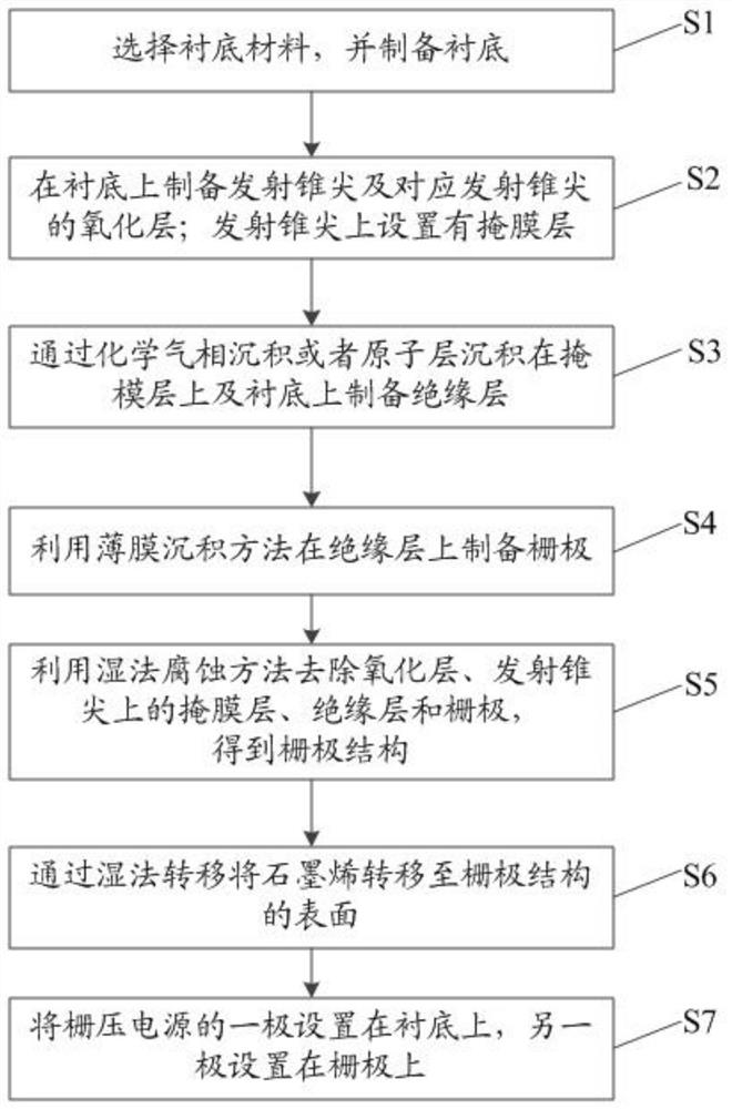
[0055] The following will clearly and completely describe the technical solutions in the embodiments of the present invention with reference to the accompanying drawings in the embodiments of the present invention. Obviously, the described embodiments are only some of the embodiments of the present invention, not all of them. Based on the embodiments of the present invention, all other embodiments obtained by persons of ordinary skill in the art without making creative efforts belong to the protection scope of the present invention.
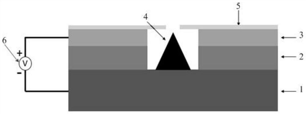
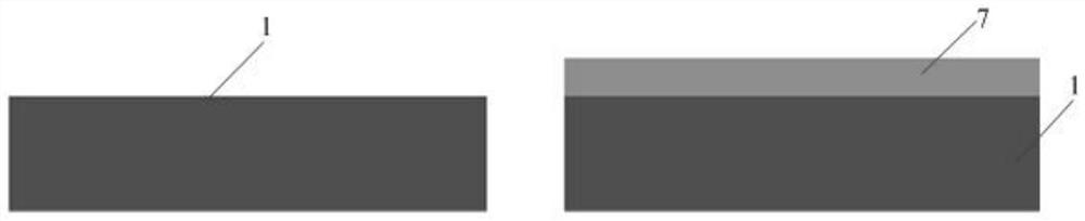
[0056] The object of the present invention is to provide a self-aligned graphene field emission grid structure, including a bottom-up substrate, emission cone tip, insulating layer, grid and graphene; On the bottom, the other pole is added to the gate. By applying a small gate voltage between the substrate and the gate, a greatly enhanced electric field can be formed at the tip, so that the emission cone emits electrons. By changing the magnitude...
PUM
| Property | Measurement | Unit |
|---|---|---|
| Height | aaaaa | aaaaa |
Abstract
Description
Claims
Application Information