Multi-layer wave absorber structure and application thereof
A wave absorber and composite wave-absorbing material technology, applied in antennas, screening casings, electrical components, etc., can solve the problems of high total mass of wave absorbers, limited practical applications, and lack of universality of interlayers, and achieve improvement The effect of effective absorption bandwidth, strong universality and operability, and strong application value
- Summary
- Abstract
- Description
- Claims
- Application Information
AI Technical Summary
Problems solved by technology
Method used
Image
Examples
Embodiment 1
[0054] (1) Single-layer graphene absorber: metal backing and graphene-paraffin composite absorbing material on metal backing surface.
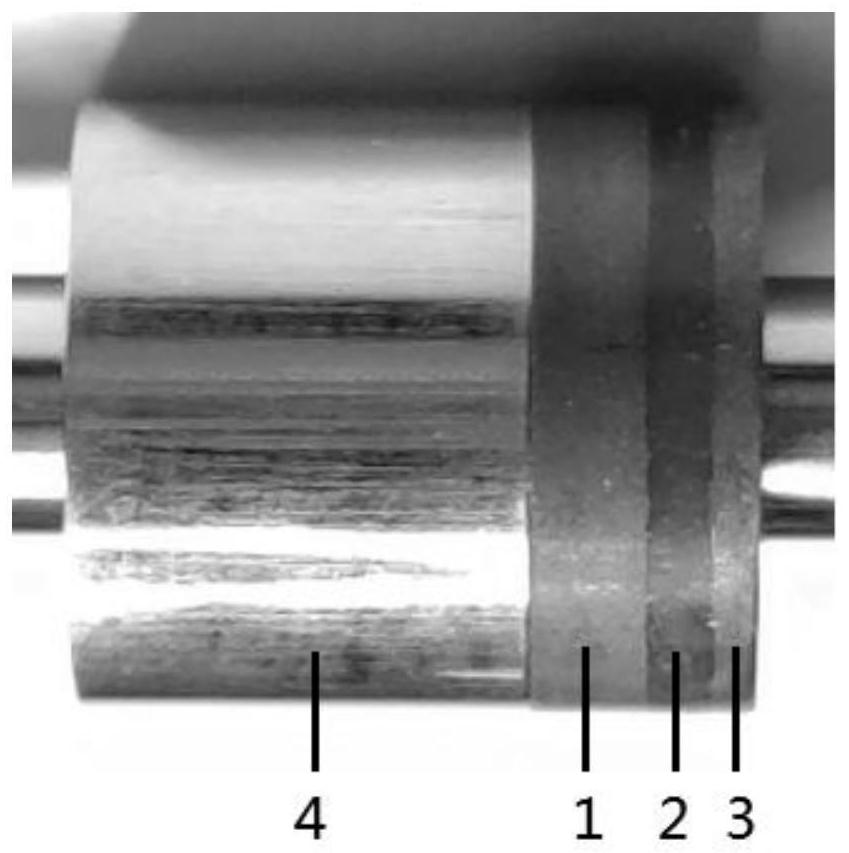
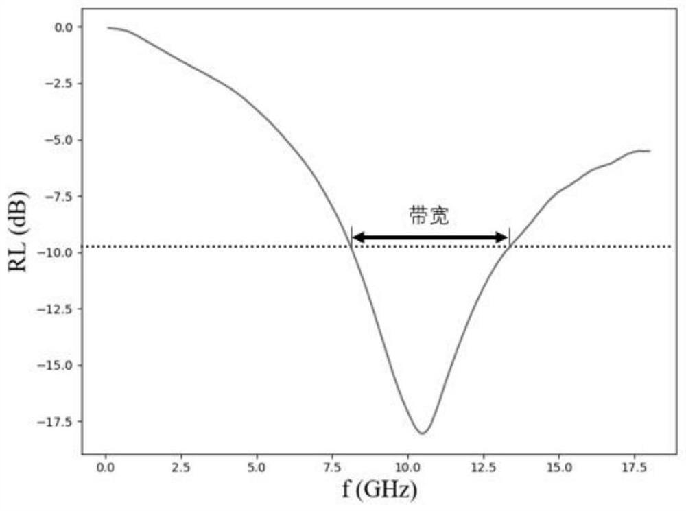
[0055] After dissolving paraffin in n-hexane, add graphene powder, centrifuge and stir until n-hexane volatilizes to obtain a uniformly mixed graphene-paraffin composite absorbing material (the mass ratio of graphene and paraffin is 3:8), and the graphene-paraffin The composite absorbing material is placed in a mold and pressed to obtain a cylindrical ring with an inner diameter of 3.04 mm and an outer diameter of 7.00 mm. Measure the electromagnetic parameters of the cylindrical ring on the Agilent vector network analyzer, and calculate the electromagnetic wave reflection loss curves of the cylindrical rings with different thicknesses according to the electromagnetic parameters. The results are as follows Figure 4 As shown in (a), according to Figure 4 In (a), it can be seen that the best effective absorption bandwidth that the single-laye...
Embodiment 2
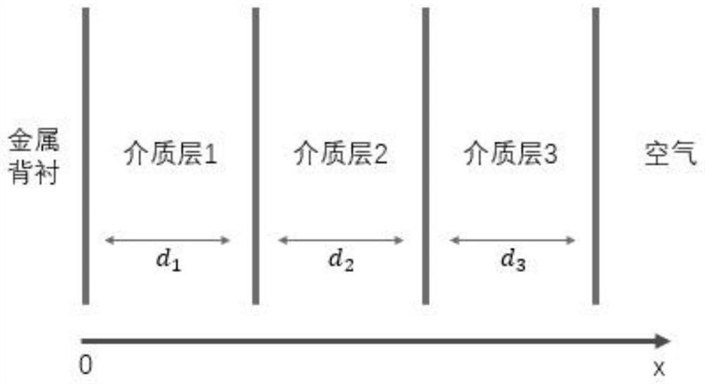
[0059] Carry out the theoretical calculation reflection loss curve of the multilayer wave absorber structure according to the method of embodiment 1 steps (1)~(2), and the difference with embodiment 1 is that the non-electromagnetic loss medium layer in step (2) has a thickness of 1.3 mm air layer, the structure of the multilayer absorber is a metal backing and a 1.4mm graphene-paraffin composite absorbing material layer, a 1.3mm air layer and a 0.3mm graphene-paraffin composite absorbing material layer stacked on the surface of the metal backing Material layer (recorded as 1.4mm+1.3mm air layer+0.3mm), the theoretically calculated reflection loss curve is as follows Figure 5 shown. Limited to the laboratory, it is currently impossible to prepare hollow samples for testing. The calculation result is not much different from that of using paraffin as the non-electromagnetic loss dielectric layer. This is because air and paraffin have similar high-frequency electromagnetic prop...
Embodiment 3
[0061] (1) Dissolve paraffin in n-hexane and add La 2 Fe 4 co 10 B powder, centrifuged until n-hexane volatilizes to obtain evenly mixed La 2 Fe 4 co 10 B-paraffin composite absorbing material (La 2 Fe 4 co 10 B and paraffin mass ratio is 5:1), the La 2 Fe 4 co 10 B-The paraffin composite wave-absorbing material is placed in a mold and pressed to obtain La with an inner diameter of 3.04mm and an outer diameter of 7.00mm. 2 Fe 4 co 10 B- paraffin cylindrical ring (denoted as single layer La 2 Fe 4 co 10 B).
[0062] (2) the La in step (1) 2 Fe 4 co 10 B is replaced by carbonyl iron, and the mass ratio of carbonyl iron and paraffin is 3:1, and a carbonyl iron-paraffin cylindrical ring (denoted as a single-layer carbonyl iron) is obtained.
[0063] (3)La 2 Fe 4 co 10 B / carbonyl iron double-layer absorber (denoted as double-layer): metal backing, 0.9mmLa stacked successively on the surface of the metal backing 2 Fe 4 co 10 B-paraffin wax composite absorbin...
PUM
| Property | Measurement | Unit |
|---|---|---|
| The inside diameter of | aaaaa | aaaaa |
| Outer diameter | aaaaa | aaaaa |
| Thickness | aaaaa | aaaaa |
Abstract
Description
Claims
Application Information


