Manufacturing method of silicon carbide micro-reaction assembly and silicon carbide micro-reaction assembly

A manufacturing method, a technology of silicon carbide, applied in chemical instruments and methods, chemical/physical/physical chemical reactors, chemical/physical/physical chemical fixed reactors, etc., can solve the problem of difficult control of micro-flow and silicon carbide micro-reactions It is difficult for components to precisely control the width and depth of microchannels, etc., to achieve precise control, good corrosion resistance, and good wettability

Active Publication Date: 2021-11-26
NANTONG SANZER PRECISION CERAMICS CO LTD
View PDF8 Cites 0 Cited by
  • Summary
  • Abstract
  • Description
  • Claims
  • Application Information

AI Technical Summary

Problems solved by technology

[0005] In order to solve the problem that the traditional manufacturing method is difficult to accurately control the width and depth of the micro-channel when manufacturing silicon carbide micro-reaction components, resulting in difficult control of the micro-flow, this application provides A method of manufacturing a silicon carbide micro-reaction component and a silicon carbide micro-reaction component

Method used


Image

  • Manufacturing method of silicon carbide micro-reaction assembly and silicon carbide micro-reaction assembly
  • Manufacturing method of silicon carbide micro-reaction assembly and silicon carbide micro-reaction assembly
  • Manufacturing method of silicon carbide micro-reaction assembly and silicon carbide micro-reaction assembly

Examples


Embodiment 1

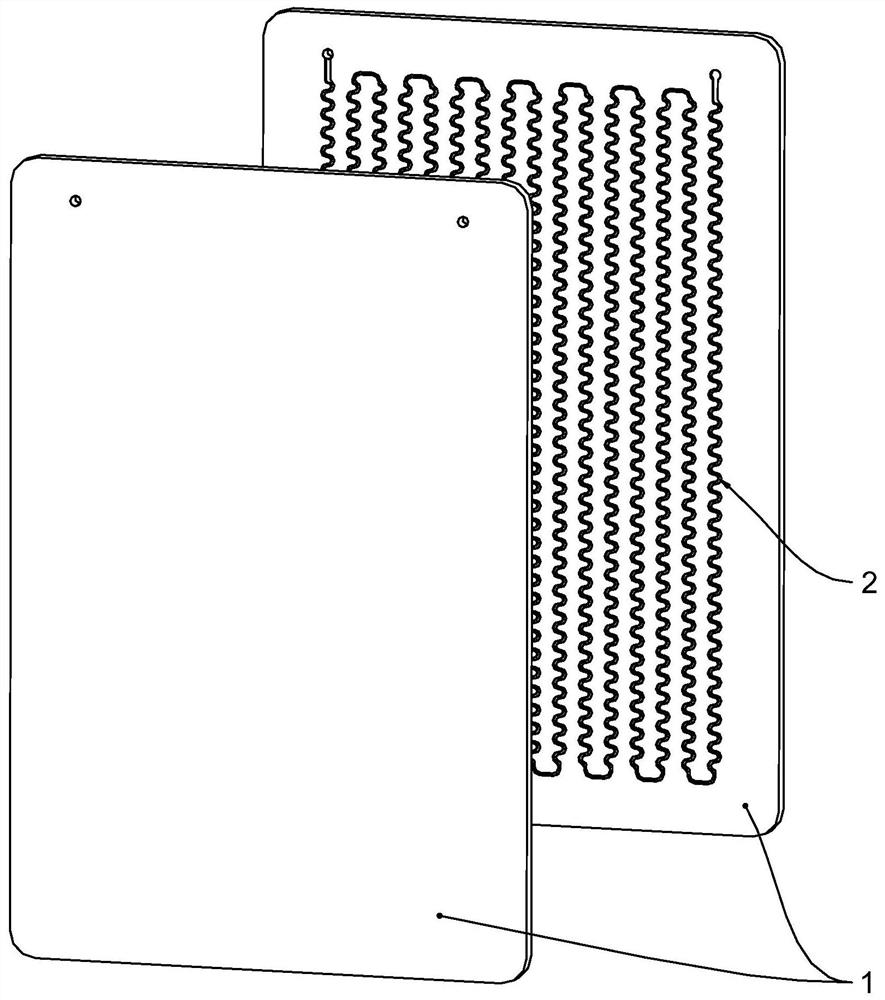
[0042] The silicon carbide micro-reaction assembly includes two reaction plates 1 (such as Figure 1-2 shown), wherein the thickness of the reaction plate 1 is 5 mm, the width of the microchannel 2 is 0.1 mm, and the depth is 0.2 mm.

[0043] The specific manufacturing steps are:

[0044] (A) Plain embryo forming: use silicon carbide to spray granulate powder, and directly isostatic pressing to obtain a green embryo;

[0045] (B) Elemental embryo processing: according to the design size, the reaction plate element embryos are processed in a plane, and the microchannels are not processed;

[0046] (C) High-temperature sintering: the plate obtained in step (B) is sintered under vacuum micro-negative pressure, and the sintering conditions are: 2100°C-2150°C, 0.5 h;

[0047] (D) Reaction plate processing: laser processing technology is used to process microchannels on the required reaction plates, the width of the microchannel is 0.1mm, the depth is 0.2mm, and the inlet and outl...

Embodiment 2

[0050] The silicon carbide micro-reaction assembly includes three reaction plates 1 and two heat exchange plates 3 (such as Figure 3-4 The thickness of the reaction plate 1 in the middle is 8 mm, the thickness of the two reaction plates 1 on both sides is 10 mm, the width of the microchannel 2 is 0.6 mm, the depth is 0.8 mm, and the thickness of the heat exchange plate 3 The width of the heat exchange medium channel 4 is 9 mm and the depth is 3 mm. It is used between the reaction plate 1 and between the reaction plate 1 and the heat exchange plate 3. The welding temperature is 1400 ℃, and the welding pressure is 10 bar.

[0051] The specific manufacturing steps are:

[0052] (A) Plain embryo forming: use silicon carbide to spray granulate powder, and directly isostatic pressing to obtain a green embryo;

[0053] (B) Preform processing: according to the design size, the reaction plate blank is processed on a plane without processing microchannels; according to the design siz...

Embodiment 3

[0060] The silicon carbide micro-reaction assembly includes two reaction plates 1 (such as Figure 1-2 shown), the thickness of reaction plate 1 is 8 mm, the width of microchannel 2 is 0.8 mm, and the depth is 1 mm.

[0061] Ni-Fe-Cr-Mo Hastelloy foils with a thickness of 0.1 mm are used for welding between the two reaction plates 1 at a welding temperature of 1350 °C and a welding pressure of 30 bar.

[0062] The specific manufacturing steps are:

[0063] (A) Plain embryo forming: use silicon carbide to spray granulate powder, and directly isostatic pressing to obtain a green embryo;

[0064] (B) Elemental embryo processing: according to the design size, the reaction plate element embryos are processed in a plane, and the microchannels are not processed;

[0065] (C) High temperature sintering: the plate obtained in step (B) is sintered under vacuum micro-negative pressure, and the sintering conditions are: 2100°C-2150°C, 1 h;

[0066] (D) Reaction plate processing: The mi...


PUM

PropertyMeasurementUnit
widthaaaaaaaaaa
depthaaaaaaaaaa
thicknessaaaaaaaaaa

Abstract

The invention belongs to the technical field of micro-reaction assemblies, and particularly relates to a manufacturing method of a silicon carbide micro-reaction assembly and the silicon carbide micro-reaction assembly. The manufacturing method of the silicon carbide micro-reaction assembly comprises the following steps of (A) blank forming: adopting silicon carbide spray granulation powder, and directly performing isostatic pressing forming to obtain a blank, (B) plain blank processing: carrying out plane processing on the reaction plate plain blank according to a design size without processing a micro-channel, (C) high-temperature sintering: carrying out vacuum micro-negative pressure sintering on the plate obtained in the step (B), (D) processing a reaction plate: processing a micro-channel on the required reaction plate by laser, and carrying out finish machining on the feeding and discharging hole and the positioning hole, and (E) high-temperature welding: fixing the corrosion-resistant Hastelloy alloy foil between adjacent plates, and welding at the temperature of 1300-1400 DEG C and the pressure of 10-50 bar. The micro-channel of the reaction plate is obtained through laser processing after high-temperature sintering, accurate control can be achieved under the condition that the size of the micro-channel is very small, and micro-flow control is facilitated.

Description

technical field [0001] The application belongs to the technical field of micro-reaction components, and in particular relates to a manufacturing method of a silicon carbide micro-reaction component and a silicon carbide micro-reaction component. Background technique [0002] Due to its inherent safety characteristics, microreactors have high reaction efficiency, which greatly promotes the reliability of chemical reactions. However, for the reaction involving strong acid and alkali, traditional metal materials and glass materials cannot adapt to the reaction conditions, and silicon carbide materials with excellent corrosion resistance are required. For reactions at high temperature and high pressure, the fabrication of silicon carbide microreaction assemblies is particularly critical. Especially for some catalytic reactions, the reaction channel is required to be very narrow, usually within 0.5mm, or even about 0.2mm, which is usually difficult to achieve for silicon carbide...

Claims


Application Information

Patent Timeline
Patent Type & Authority Applications(China)
IPC IPC(8): C04B35/565C04B35/622C04B37/00C04B41/91B01J19/00B01J19/24
CPCC04B35/565C04B35/622C04B41/5346C04B41/91C04B37/003B01J19/0093B01J19/0053B01J19/24C04B2235/602C04B2235/612C04B2235/6581C04B2235/656C04B2235/6567C04B2237/122
Inventor 闫永杰姚玉玺
Owner NANTONG SANZER PRECISION CERAMICS CO LTD
Why Eureka
Try Eureka