
Broadband wide-angle anti-reflection composite micro-nano structure surface and preparation method thereof

A micro-nano structure and anti-reflection technology, which is applied in the field of optical technology and micro-nano processing, can solve the problems of decreased transmittance and inability to maintain the anti-reflection effect

Active Publication Date: 2021-12-03
CHANGCHUN UNIV OF SCI & TECH
View PDF4 Cites 2 Cited by
  • Summary
  • Abstract
  • Description
  • Claims
  • Application Information

AI Technical Summary

Problems solved by technology

The moth-eye micro-nano structure can achieve the ideal broadband anti-reflection effect, but as the angle requirements increase, such as 70-80°, even the transmittance of the moth-eye structure will drop significantly, and it cannot maintain a good anti-reflection effect effect
To maintain a large-angle transmittance of 70-80°, it is necessary to increase the structural height and aspect ratio of the moth-eye micro-nano structure, which poses a severe challenge to the micro-nano processing technology

Method used


Image

  • Broadband wide-angle anti-reflection composite micro-nano structure surface and preparation method thereof
  • Broadband wide-angle anti-reflection composite micro-nano structure surface and preparation method thereof
  • Broadband wide-angle anti-reflection composite micro-nano structure surface and preparation method thereof

Examples


Embodiment Construction

[0053] The present invention will be described in further detail below in conjunction with the accompanying drawings.

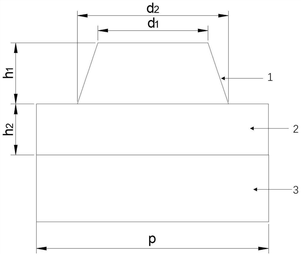
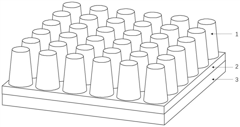
[0054] Such as Figure 1-2 As shown, a wide bandwidth angle anti-reflection composite micro-nano structure surface, which forms a single-layer optical film on the surface of the optical material substrate, and forms a certain depth of micro-nano structure on the film layer; its structure includes: micro-nano structure layer 1 , middle residual layer 2 and base layer 3 .

[0055] The micro-nano structural units are cylindrical, conical, conical, Gaussian or parabolic, etc. The shape of the unit is optimized according to the incident spectral segment and bandwidth, as well as the range of incident angles. height h 1 , top diameter d 1 , bottom diameter d 2 to describe. The equation of the micro-nano structural unit in the three-dimensional Cartesian coordinate system is: Where x, y, z represent the three-dimensional coordinates of a point on the surface ...


PUM

PropertyMeasurementUnit
diameteraaaaaaaaaa
heightaaaaaaaaaa
diameteraaaaaaaaaa

Abstract

The invention discloses a broadband wide-angle composite micro-nano structure anti-reflection surface, belongs to the technical field of optical technology and micro-nano machining, and aims to overcome the defects that in the bionic moth eye micro-nano structure surface technology, the structure height and the depth-to-width ratio restrict the micro-nano machining technology, and in the optical anti-reflection film technology, the anti-reflection performance is limited by the incident angle. A single-layer thin film is formed on the surface of an optical material substrate, a moth eye micro-nano structure with a certain depth is formed on a thin film layer, a residual film layer is reserved, and is composed of three basic structures which sequentially comprise a micro-nano structure layer, a middle residual layer and a substrate layer. The micro-nano structure layer is composed of a micro-nano structure unit array, and the cycle of the micro-nano structure unit meets the sub-wavelength transmission requirement under the condition of the designed incident angle, namely, lambda min represents the minimum incident wavelength, nsub represents the refractive index of the substrate, n0 represents the refractive index of air, theta max represents the maximum incident angle, and p represents the cycle of the micro-nano structure unit. According to the invention, the imaging quality is not influenced while the high transmittance is ensured.

Description

technical field [0001] The invention relates to an anti-reflection composite micro-nano structure surface with wide bandwidth and angle and a preparation method thereof, belonging to the technical fields of optical technology and micro-nano processing. Background technique [0002] Anti-optical reflection performance is an important interface feature to improve the energy utilization rate of optical components and reduce stray light. The commonly used anti-reflection window is coated with a single layer or multiple layers of dielectric films with different refractive indices on the surface of the substrate, and the light is reflected multiple times in the film, resulting in interference phenomenon. When the wavelength of the incident light, the thickness of the film and the refractive index of the film meet the conditions of destructive interference, the transmittance of light energy is the largest, achieving the purpose of anti-reflection. Traditional anti-reflection optic...

Claims


Application Information

Patent Timeline
Patent Type & Authority Applications(China)
IPC IPC(8): G02B1/118C23C14/06C23C14/24C23C14/35C23C14/16C25D1/10C23C16/40C23C16/455
CPCG02B1/118C23C14/0623C23C14/24C23C14/35C23C14/165C25D1/10C23C16/403C23C16/45525Y02P70/50
Inventor 欧阳名钊张自强付跃刚任航张凯刘智颖张磊胡源王加科
Owner CHANGCHUN UNIV OF SCI & TECH
Learn More