Mask, manufacturing method of array substrate, and display panel

A technology of array substrate and mask, which is applied in the field of display panel preparation, can solve the problems of critical size loss and large difference in parasitic capacitance Cgs, etc., and achieve the effects of reducing size loss, improving picture quality, and ensuring processing size

Inactive Publication Date: 2021-12-07
HKC CORP LTD
View PDF10 Cites 0 Cited by
  • Summary
  • Abstract
  • Description
  • Claims
  • Application Information

AI Technical Summary

Problems solved by technology

At present, the switch design of TFT adopts four photolithography process (4mask) design, the peripheral position of the source level needs to be etched twice in the etching process, and its critical dimension will be greatly lost, generally in the range of 1um to 2um, and due to the two times of etching Due to the difference in liquid and etching time, the size loss of the source of the TFT switch in different display areas is quite different, resulting in a large difference in the parasitic capacitance Cgs in different places

Method used


Image

  • Mask, manufacturing method of array substrate, and display panel
  • Mask, manufacturing method of array substrate, and display panel
  • Mask, manufacturing method of array substrate, and display panel

Examples


Embodiment 1

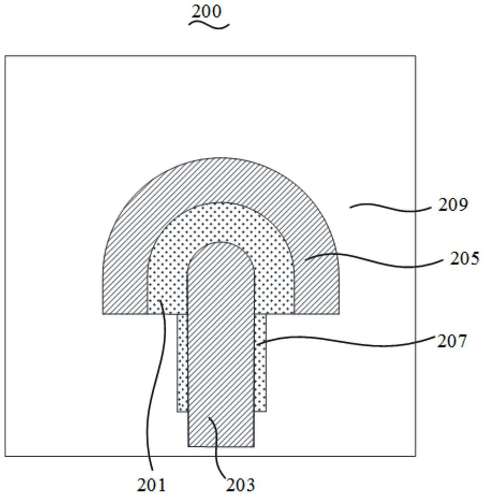
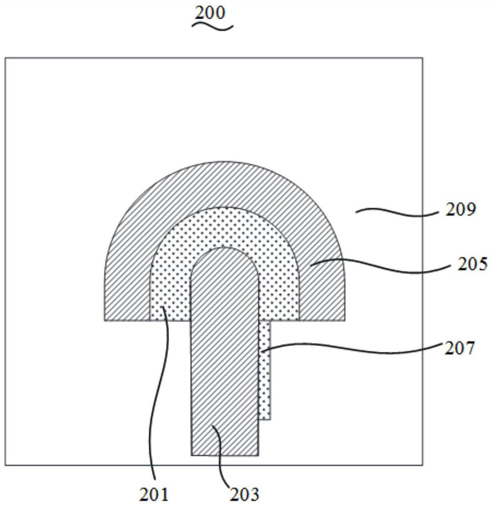
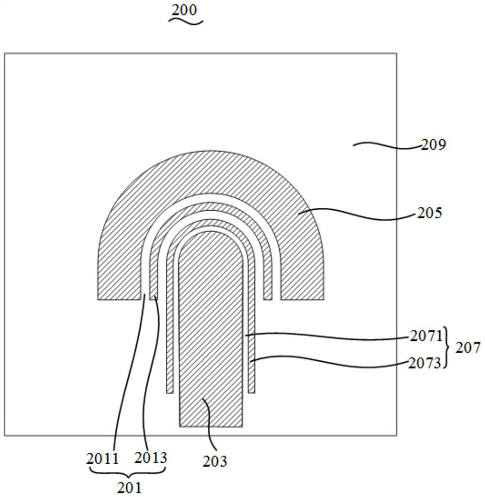
[0040] The present invention provides a mask plate 200 for making an array substrate.

[0041] Please refer to Figure 1 to Figure 4 , it can be seen that the array substrate includes a thin film transistor, and the thin film transistor includes a gate, a source 51 and a drain 53 arranged at intervals, and a channel region 41 is formed between the source 51 and the drain 53 . The mask plate 200 includes: a first exposure region 201 corresponding to the channel region 41 , a second exposure region 203 on one side of the first exposure region 201 where the source electrode 51 is to be formed, and a second exposure region 203 on the side of the first exposure region 201 . The third exposure area 205 where the drain electrode 53 is to be formed on the opposite side of the exposure area 201, and the fourth exposure area 207 located at the edge of the second exposure area 203 that does not overlap with the first exposure area 201 , both the first exposure area 201 and the fourth ex...

Embodiment 2

[0070] Please refer to Figure 5 to Figure 9 , the present invention also provides a method for manufacturing an array substrate using the mask plate of any one of the above embodiments, the method includes the following steps:

[0071] Please combine Figure 6 , step S1: provide a substrate 10, and sequentially form a gate 20, a gate insulating layer 30, a semiconductor layer 40, a metal layer 50 and a photoresist layer on the substrate 10 from bottom to top, and the semiconductor layer 40 corresponds to the A channel region 41 is provided at the position of the gate 20 .

[0072] It can be understood that the array substrate 100 is a multi-layer structure, and each layer structure is formed layer by layer through coating, exposure, development and etching processes, which can be completed through four photolithography (4MASK) processes. Specifically, the array substrate 100 includes a base 10 , which provides a basic carrier. The base 10 is transparent, and its material ma...

Embodiment 3

[0087] Please refer to Figure 10 The present invention also proposes a display panel 300, the display panel 300 includes a color filter substrate 400, an array substrate 100, and a liquid crystal layer 500, the color filter substrate 400 and the array substrate 300 are arranged in pairs, and the array substrate 100 It is prepared by adopting the manufacturing method of the array substrate as described in any of the above embodiments. Since the display panel 300 includes all the technical solutions of all the above-mentioned embodiments, it at least has all the beneficial effects brought by the technical solutions of the above-mentioned embodiments, and will not be repeated here.

[0088] recombine Figure 4 and Figure 9, wherein the array substrate 100 includes a base 10 and a gate 20, an active layer 43, a drain 53, and a source 51 sequentially disposed on the base 10, and the edges of the channel region 41 and the source 51 of the semiconductor layer 40 are masked. The ...


PUM

PropertyMeasurementUnit
widthaaaaaaaaaa
widthaaaaaaaaaa
transmittivityaaaaaaaaaa

Abstract

The invention discloses a mask, a manufacturing method of an array substrate, and a display panel. The mask comprises: a first exposure region corresponding to the channel region, a second exposure region which is positioned on one side of the first exposure region and is about to form a source electrode, a third exposure region which is positioned on the other side opposite to the first exposure region and is about to form a drain electrode, a fourth exposure area which is located on the partial edge of the second exposure area and is not overlapped with the first exposure area, wherein the first exposure area and the fourth exposure area are both semi-transparent areas. According to the technical scheme, in the exposure and development process of the mask, part of light resistance can be left in the areas corresponding to the first exposure area and the fourth exposure area, and a channel area to be formed and an area to be formed with a source electrode are protected, so that the processing size of the source electrode is guaranteed, and the stability of stray capacitance formed by the source electrode and the grid electrode is improved.

Description

technical field [0001] The invention relates to the technical field of display panel preparation, in particular to a mask plate, a method for manufacturing an array substrate and a display panel. Background technique [0002] Since the thin film transistor liquid crystal display (Thin film transistor liquid crystal display, TFT-LCD) has the advantages of low radiation, small size, low energy consumption, etc., it is widely used in various electronic information products. With the development of science and technology, the market has higher and higher requirements for the quality of TFT-LCD. Improving the taste of the display screen is the key to improving the quality. Among them, the parasitic capacitance Cgs between the source and gate in the TFT switch design has a great impact on the display screen. Taste matters. At present, the switch design of TFT adopts four photolithography process (4mask) design, the peripheral position of the source level needs to be etched twice ...

Claims


Application Information

Patent Timeline
Patent Type & Authority Applications(China)
IPC IPC(8): G03F1/32
CPCG03F1/32
Inventor 王光加黄世帅袁海江
Owner HKC CORP LTD
Why Eureka
Try Eureka