

Synchronous rectification control circuit
Patent Information
- Authority / Receiving Office
- CN · China
- Current Assignee / Owner
- MORNSUN GUANGZHOU SCI & TECH
- Publication Date
- 2021-12-17
Smart Images
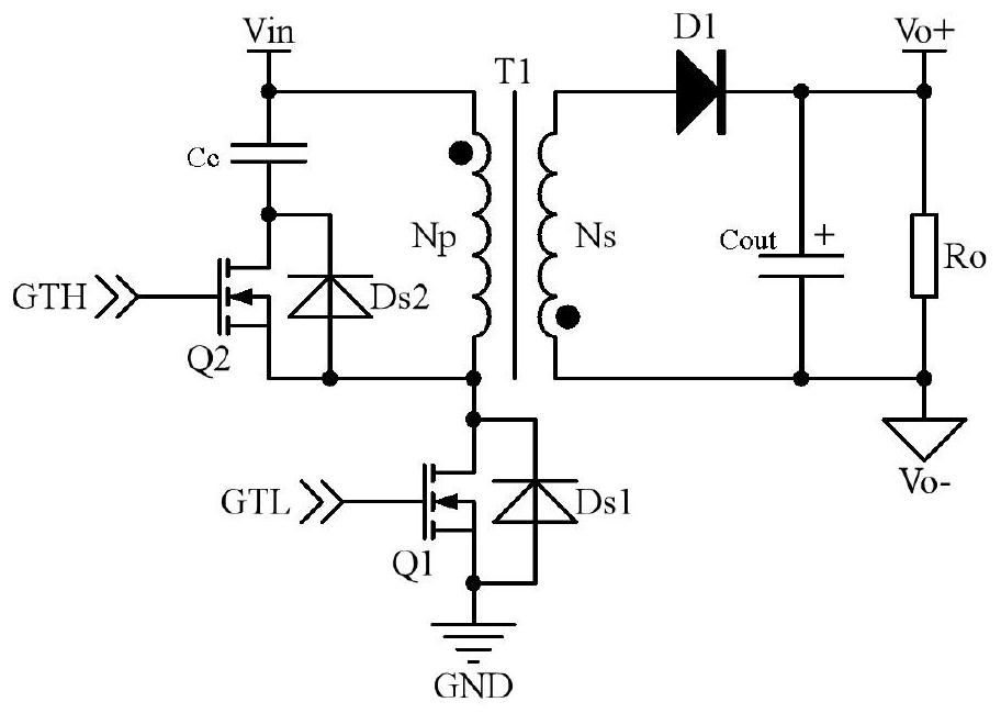
Figure 1 
Figure 2 
Figure 3
Abstract
Description
technical field
[0001] The invention relates to the field of switching converters, in particular to the synchronous rectification control of active clamp flyback switching converters. Background technique
[0002] Active clamp flyback (Active Clamp Flyback, ACF) converter is a kind of flyback converter, which has a main switch tube that can realize zero voltage turn-on (ZVS), leakage inductance can be absorbed without loss, and the voltage spike of the main switch tube is small , high efficiency and other advantages, the application is more and more extensive. The circuit schematic diagram of the existing conventional active clamp flyback converter is as follows: figure 1 , figure 1 Among them, Q1 is the main switching tube (hereinafter referred to as the supervisor), Q2 is the clamping switching tube (hereinafter referred to as the clamping tube), Cc is the clamping capacitor; Ds1 is the body diode of the main switching tube Q1, and Ds2 is the clamping switching tube bod...