Charge plasma SiGe heterojunction bipolar transistor

A heterojunction bipolar and plasma technology, applied in circuits, electrical components, semiconductor devices, etc., can solve the problems of reduced breakdown voltage, increased electron concentration, unfavorable application of charge plasma bipolar transistors, etc., to achieve Increase the current gain, improve the breakdown voltage, the effect of synchronously increasing the current gain and the breakdown voltage

Pending Publication Date: 2021-12-24
BEIJING UNIV OF TECH
View PDF3 Cites 0 Cited by
  • Summary
  • Abstract
  • Description
  • Claims
  • Application Information

AI Technical Summary

Problems solved by technology

However, the electron concentration on one side of the collector region will also increase accordingly, and the breakdown voltage will be greatly reduced at this time, which is not conducive to the application of charge plasma bipolar transistors in high-speed hybrid analog integrated circuits

Method used


Image

  • Charge plasma SiGe heterojunction bipolar transistor
  • Charge plasma SiGe heterojunction bipolar transistor
  • Charge plasma SiGe heterojunction bipolar transistor

Examples


Embodiment Construction

[0017] In the embodiment of the present invention, a charge plasma SiGe heterojunction bipolar transistor with a Ge component content of 0.1 is taken as an example to describe the content of the present invention in detail. The field to which the present invention relates is not limited thereto.

[0018] Implementation example:

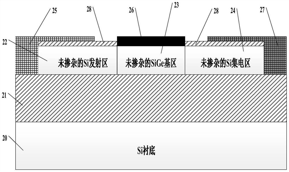
[0019] The charge plasma SiGe heterojunction bipolar transistor disclosed in the embodiment of the present invention, figure 2 Illustrates its longitudinal cross-sectional schematic diagram, including Si substrate (20), thickness is 25nm; SiO 2 Buried oxide layer (21), thickness is 25nm; Undoped SiGe base region (23), Ge composition is 0.1, and thickness is 15nm, and width is 60nm; Undoped Si emitter region (22) and undoped The Si collector region (24) has a thickness of 15nm and a width of 70nm; wherein the undoped SiGe base region (23), Si emitter region (22) and Si collector region (24) are located on SiO 2 Above the buried oxide layer (21); Si...


PUM

PropertyMeasurementUnit
thicknessaaaaaaaaaa
thicknessaaaaaaaaaa
widthaaaaaaaaaa

Abstract

The invention discloses a charge plasma SiGe heterojunction bipolar transistor, which is an npn type transistor. A base region is prepared by adopting a SiGe material, a heterojunction is formed by the base region, an undoped Si emitter region and a Si collector region, and the current gain of the device is improved by effectively changing an energy band structure at an emitter junction. Meanwhile, due to the fact that the work function of cadmium metal is 4.07 eV, the cadmium metal can easily form good gold-semi-contact with undoped Si, n-type charge plasma is effectively induced to be generated, and the transistor has the advantages of being excellent in conductivity, welding resistance, tensile strength and abrasion resistance and the like; therefore, cadmium metal is used as an electrode material of the emitter and the collector and is used for adjusting the concentration of n-type carriers in the corresponding emitter region and the collector region below the emitter and the collector. Through effective cooperation of the above structure, synchronous improvement of transistor current gain, breakdown voltage and characteristic frequency is realized.

Description

technical field [0001] The invention relates to a charge plasma SiGe heterojunction bipolar transistor, in particular to a charge plasma SiGe heterojunction bipolar transistor suitable for the fields of display drive circuits, high-speed mixed signals, and low-power wireless integrated circuits. Background technique [0002] Compared with traditional silicon-on-insulator (SOI)-based bipolar transistors, charge plasma bipolar transistors do not require a doping process, and only use metal materials with different work functions as electrodes to form good gold- Semi-contact can effectively induce charge plasma to form a bipolar transistor. Therefore, it has the advantages of simple preparation process, no need for doping and thermal annealing, and is compatible with mature CMOS processes. It will be used in the field of high-speed hybrid analog integrated circuits play an increasingly important role. [0003] figure 1 A schematic diagram showing a longitudinal section of a c...

Claims


Application Information

Patent Timeline
Patent Type & Authority Applications(China)
IPC IPC(8): H01L29/737H01L29/735H01L29/06H01L29/45
CPCH01L29/737H01L29/735H01L29/0603H01L29/456
Inventor 金冬月贾晓雪张万荣曹路明刘圆圆
Owner BEIJING UNIV OF TECH
Why Eureka
Try Eureka