Wavelength demultiplexing device based on on-chip super lens structure

A super-lens and demultiplexing technology, applied in the field of integrated optoelectronics, can solve the problems of complex structure and large size, and achieve the effect of easy integration, low loss, and high-density integrated planar optical circuit chip on chip

Active Publication Date: 2022-01-04
SHANGHAI JIAO TONG UNIV +1
View PDF7 Cites 5 Cited by
  • Summary
  • Abstract
  • Description
  • Claims
  • Application Information

AI Technical Summary

Problems solved by technology

[0005] In order to overcome the deficiencies of the above-mentioned prior art, the present invention provides a wavelength demultiplexing device based on an on-chip metalens structure, which solves the problem of the traditional wavelength demultiplexing device size Large, complex problems

Method used


Image

  • Wavelength demultiplexing device based on on-chip super lens structure
  • Wavelength demultiplexing device based on on-chip super lens structure
  • Wavelength demultiplexing device based on on-chip super lens structure

Examples


Embodiment Construction

[0024] The specific implementation manner of the present invention will be described in detail below in conjunction with the accompanying drawings and preferred embodiments.

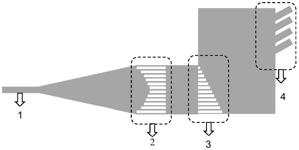
[0025] Such as figure 1 As shown, the present invention is based on a wavelength demultiplexing device with an on-chip metalens structure, and adopts a technical solution of etching a metalens whose structural unit is a rectangular groove on a silicon-based waveguide to realize the separation of wavelength-multiplexed light waves, namely Achieve wavelength demultiplexing. Specifically, it includes an input waveguide 1, the input waveguide 1 is connected to a collimating metalens 2②, ​​the collimating metalens 2 is connected to a dispersion-focusing metalens 3, and the dispersion-focusing metalens 3 is connected to an output waveguide array 4. The input waveguide 1 is used to transmit the input light wave, the collimating metalens 2 is used to change the input light wave into a plane wave, and the dispe...


PUM


Abstract

The invention discloses a wavelength demultiplexing device based on an on-chip super lens structure. The wavelength demultiplexing device comprises an input waveguide, a collimating super lens, a dispersion focusing super lens and an output waveguide array, light entering from the input waveguide is changed into parallel light through the collimation super lens, and the parallel light is deflected through the dispersion focusing super lens and is focused and coupled to the output waveguide array. Light with different wavelengths has different deflection angles after passing through the dispersion focusing super lens, so that the light can enter output waveguides at different positions, and wavelength demultiplexing is realized. According to the invention, a super-lens structure is adopted to flexibly control a light wave phase plane, a super-compact wavelength demultiplexer can be realized, and silicon substrate integration is easy.

Description

technical field [0001] The invention relates to the technical field of integrated optoelectronics, in particular to a wavelength demultiplexing device based on an on-chip super-lens structure. Background technique [0002] It has always been a dream of people to realize flexible control of light. In recent years, researchers have proposed a concept of a metalens composed of sub-wavelength micro-nano structures, which can flexibly control light, and has been verified experimentally. Based on this idea, the research of metalens has also made a lot of progress. Compared with traditional lenses, metalenses are more flexible in regulating light, can realize light regulation in a shorter distance, and have a smaller volume, which is conducive to the integration of optical components. In addition, the metalens can also break through the diffraction limit to focus the light beam. Since the metalens is a planar element, it fundamentally solves the aberration problem of the tradition...

Claims


Application Information

Patent Timeline
Patent Type & Authority Applications(China)
IPC IPC(8): G02B6/293
CPCG02B6/2938G02B6/29302
Inventor 周林杰冉诗环陆梁军陈建平刘娇
Owner SHANGHAI JIAO TONG UNIV
Why Eureka
Try Eureka