
Method for controlling direct-writing photoetching machine and direct-writing photoetching machine

A lithography machine and direct-write technology, applied in the field of data processing, can solve the problems of slow processing speed, long processing time, and inability to use data effectively, so as to shorten the processing time and improve the processing speed.

Pending Publication Date: 2022-01-14
HEFEI CHIP FOUND MICROELECTRONICS EQUIP CO LTD
View PDF0 Cites 0 Cited by
  • Summary
  • Abstract
  • Description
  • Claims
  • Application Information

AI Technical Summary

Problems solved by technology

[0003] In related technologies, in the process of repeated processing of data, the processing time is long, which easily leads to slow processing speed, and with the field of direct writing lithography becoming more and more refined and the requirements of high-end plate making, the more complex and complex the plate making circuit. Fine, the more graphics units contained in a unit area are distributed, so the data processed each time cannot be effectively used, and hardware acceleration alone cannot meet the production capacity needs of direct-write lithography machines

Method used


Image

  • Method for controlling direct-writing photoetching machine and direct-writing photoetching machine
  • Method for controlling direct-writing photoetching machine and direct-writing photoetching machine
  • Method for controlling direct-writing photoetching machine and direct-writing photoetching machine

Examples


Embodiment Construction

[0033] Embodiments of the present invention are described in detail below, and the embodiments described with reference to the drawings are exemplary, and embodiments of the present invention are described in detail below.

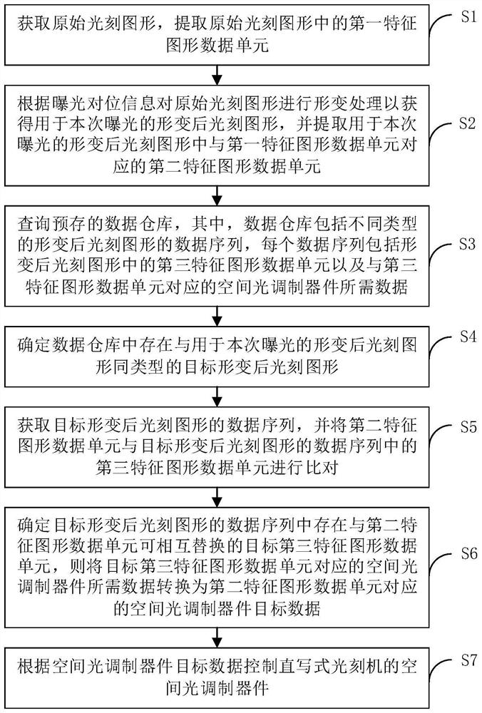
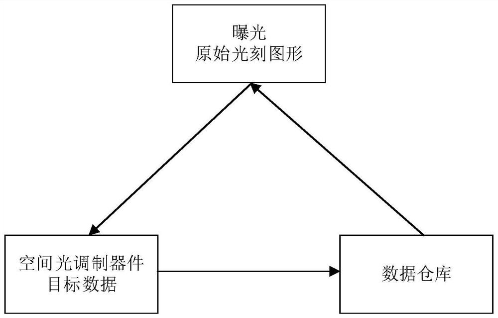
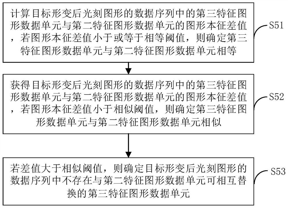
[0034] Refer below figure 1 - Figure 4 A method of controlling a direct write photolithography machine according to an embodiment of the present invention is described.

[0035] In some embodiments of the present invention, the direct writing lithography machine includes a spatial light modulation device, wherein the spatial light modulation device can use a DMD (Digital Micromirror Device, digital micromirror device) device or an LCLV (Liquid Crystal Light Valve, liquid crystal light Valve) or other suitable digital optical spatial light modulators for realizing the modulation of light.

[0036] Such as figure 1 Shown is a flow chart of a method for controlling a direct-write lithography machine according to an embodiment of the present invention. The...


PUM


Abstract

The invention discloses a method for controlling a direct-writing photoetching machine and the direct-writing photoetching machine. The direct-writing photoetching machine comprises a spatial light modulator. The method comprises the following steps of acquiring an original photoetching pattern, obtaining a deformed photoetching pattern for current exposure, and extracting a second feature pattern data unit in the deformed photoetching pattern, querying a pre-stored data warehouse, determining that the same type of target deformed photoetching patterns exist in the data warehouse, comparing the second feature pattern data unit with a third feature pattern data unit in the data sequence, determining that a target third feature pattern data unit which can be mutually replaced with the second feature pattern data unit exists, and converting data required by the corresponding spatial light modulator into spatial light modulator target data corresponding to the second feature pattern data unit, and controlling a spatial light modulator of the direct-writing photoetching machine. According to the method for controlling the direct-writing photoetching machine, the processing time is short, data processing can be realized through software, and the productivity of the direct-writing photoetching machine is improved.

Description

technical field [0001] The invention relates to the technical field of data processing, in particular to a method for controlling a direct-write photolithography machine and a direct-write photolithography machine. Background technique [0002] Direct-write lithography is a technology that prints characteristic patterns on the surface of photosensitive materials such as glue or film. Maskless lithography generally uses digital micromirror systems to generate patterns. Through optical projection components, images are projected at a certain magnification onto a light-sensitive substrate, producing a pattern of features. For semiconductor masks and wafer-level packaging and other fields, packaging substrates, class substrates, HDI (High Density Interconnector, high-density interconnect) and mSAP (Modified) for the PCB (Printed Circuit Board, printed circuit board) industry Semi-Additive Process, ultra-thin copper-skinned analog SAP method) and other processes, the production ...

Claims


Application Information

Patent Timeline
IPC IPC(8): G03F7/20
CPCG03F7/2051G03F7/70383G03F7/70491G03F7/70508
Inventor 赵美云
Owner HEFEI CHIP FOUND MICROELECTRONICS EQUIP CO LTD
Learn More