Preparation method of lithium niobate crystal domain structure and photoelectric device
A technology for optoelectronic devices, lithium niobate, applied in crystal growth, chemical instruments and methods, single crystal growth, etc., can solve the high requirements of processing technology, polarization conditions, etc., difficult to prepare PPLN structure, difficult to accurately control domain structure period problems such as sexual conditions, to achieve the effect of low sample structure requirements
- Summary
- Abstract
- Description
- Claims
- Application Information
AI Technical Summary
Problems solved by technology
Method used
Image


Examples
preparation example Construction
[0050] One aspect of the present invention provides a method for preparing a lithium niobate crystal domain structure, comprising the following steps:
[0051] Scanning the surface of the lithium niobate crystal with a voltage-applied conductive probe to form a domain structure, wherein the electric field strength formed by the conductive probe on the surface of the lithium niobate crystal is greater than or equal to the threshold electric field strength for polarization reversal of the lithium niobate crystal;
[0052] When a positive pressure is applied to the conductive probe, the scanning direction of the conductive probe is the same as the spontaneous polarization direction of the lithium niobate crystal;
[0053] When a negative pressure is applied to the conductive probe, the scanning direction of the conductive probe is opposite to the spontaneous polarization direction of the lithium niobate crystal;
[0054] Lithium niobate crystals are non-polar X-tangential or non-...
Embodiment 1
[0067] Embodiment 1 Preparation method of lithium niobate single crystal thin film domain structure
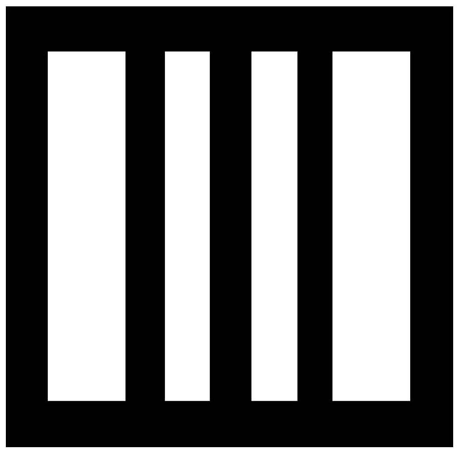
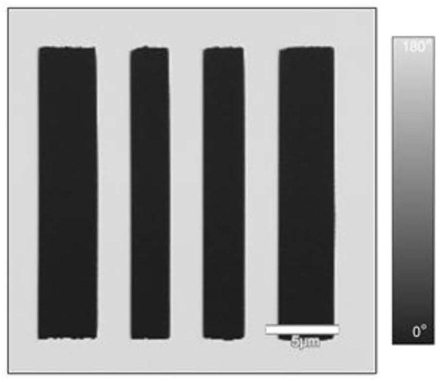
[0068] Such as figure 1 and figure 2 as shown, figure 1 (a) is a schematic diagram of the scanning direction of the domain structure prepared on the surface of the X-tangential lithium niobate single crystal film using a conductive probe after positive pressure; figure 1 (b) is a schematic diagram of the scanning direction of the domain structure prepared on the surface of the X-tangential lithium niobate single crystal film using a conductive probe after negative pressure (wherein P s is the spontaneous polarization intensity vector of lithium niobate crystal).
[0069] Place the X-tangential lithium niobate single crystal thin film on the sample stage of the atomic force microscope device, apply a voltage of 150V to the conductive probe of the atomic force microscope, and make the scanning direction of the conductive probe coincide with the X-tangential lithium niobate s...
Embodiment 2
[0070] Embodiment 2 Preparation method of lithium niobate single crystal thin film domain structure
[0071] The method for preparing the domain structure of lithium niobate single crystal thin film in Example 2 is basically the same as that in Example 1, except that a voltage of -150V is applied to the conductive probe. Specific steps are as follows:
[0072] Place the X-tangential lithium niobate single crystal thin film on the sample stage of the atomic force microscope device, apply a voltage of -150V to the conductive probe of the atomic force microscope, and make the scanning direction of the conductive probe coincide with the X-tangential lithium niobate single crystal thin film The spontaneous polarization direction is opposite, and the domain structure is prepared on the X-tangential lithium niobate single crystal film at a scanning speed of 80 μm / s. The obtained domain structure is as follows Figure 5 Shown in the middle dark area (black area). That is, at a volta...
PUM
| Property | Measurement | Unit |
|---|---|---|
| Thickness | aaaaa | aaaaa |
| Thickness | aaaaa | aaaaa |
Abstract
Description
Claims
Application Information
 - R&D
- Intellectual Property
- Life Sciences
- Materials
- Tech Scout
- Unparalleled Data Quality
- Higher Quality Content
- 60% Fewer Hallucinations
Browse by: Latest US Patents, China's latest patents, Technical Efficacy Thesaurus, Application Domain, Technology Topic, Popular Technical Reports.
© 2025 PatSnap. All rights reserved.Legal|Privacy policy|Modern Slavery Act Transparency Statement|Sitemap|About US| Contact US: help@patsnap.com