Preparation method of high-SERS-intensity Ag/SiO2 co-sputtering single-layer film
A co-sputtering, single-layer film technology, used in sputtering, coating, Raman scattering, etc., can solve the problems of insufficient sensitivity and measurement speed, limited SERS strength of single-layer metal film, etc., to improve the SERS strength. Effect
- Summary
- Abstract
- Description
- Claims
- Application Information
AI Technical Summary
Problems solved by technology
Method used
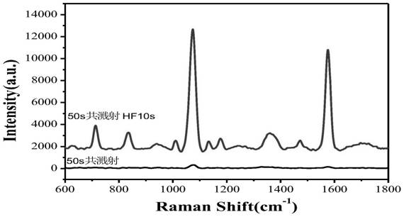
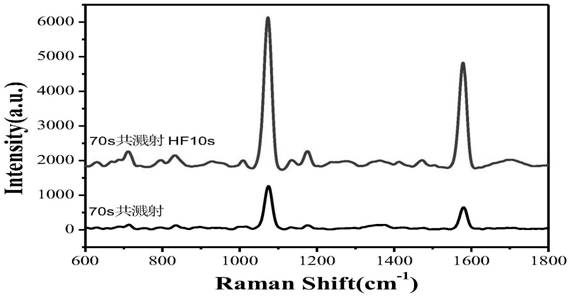
Image


Examples
Embodiment 1
[0028] (1) Hydrophilic treatment of silicon wafers: place the cleaned silicon wafers in a beaker, add ammonia water, hydrogen peroxide and deionized water to the mixed solution, in the mixed solution, the volume of ammonia water, hydrogen peroxide and deionized water The ratio is 1:2:6, keep boiling for 10-15 minutes after boiling, pour out the mixed solution after cooling, and use deionized water and absolute ethanol to repeatedly ultrasonicate the silicon wafer for 10 minutes; the silicon wafer after cleaning is made by the following steps Obtained: Soak clean silicon wafers in deionized water and absolute ethanol respectively, and ultrasonically treat them.
[0029] (2) Preparation of Ag / SiO 2 Co-sputtering single-layer film: tilt the silver target and silicon dioxide target at 40° respectively, and sputter to the silicon wafer at the same time to generate Ag / SiO on the surface of the silicon wafer 2 Co-sputtered monolayer film; the background pressure before starting is 4...
Embodiment 2
[0033] (1) Hydrophilic treatment of silicon wafers: place the cleaned silicon wafers in a beaker, add ammonia water, hydrogen peroxide and deionized water to the mixed solution, in the mixed solution, the volume of ammonia water, hydrogen peroxide and deionized water The ratio is 1:2:6, keep boiling for 10-15 minutes after boiling, pour out the mixed solution after cooling, and use deionized water and absolute ethanol to repeatedly ultrasonicate the silicon wafer for 12 minutes; the silicon wafer after cleaning is made by the following steps Obtained: Soak clean silicon wafers in deionized water and absolute ethanol respectively, and ultrasonically treat them.
[0034] (2) Preparation of Ag / SiO 2 Co-sputtering single-layer film: tilt the silver target and silicon dioxide target at 40° respectively, and sputter to the silicon wafer at the same time to generate Ag / SiO on the surface of the silicon wafer 2 Co-sputtered monolayer film; the background pressure before starting is 4...
Embodiment 3
[0038](1) Hydrophilic treatment of silicon wafers: place the cleaned silicon wafers in a beaker, add ammonia water, hydrogen peroxide and deionized water to the mixed solution, in the mixed solution, the volume of ammonia water, hydrogen peroxide and deionized water The ratio is 1:2:6. After boiling, keep boiling for 10-15 minutes. After cooling, pour out the mixed solution, and use deionized water and absolute ethanol to repeatedly sonicate the silicon wafer for 15 minutes; the silicon wafer after cleaning is prepared by the following steps: Obtained: Soak clean silicon wafers in deionized water and absolute ethanol respectively, and ultrasonically treat them.
[0039] (2) Preparation of Ag / SiO 2 Co-sputtering single-layer film: tilt the silver target and silicon dioxide target at 40° respectively, and sputter to the silicon wafer at the same time to generate Ag / SiO on the surface of the silicon wafer 2 Co-sputtered monolayer film; the background pressure before starting is ...
PUM
 Abstract
Description
Claims
Application Information
 - R&D
- Intellectual Property
- Life Sciences
- Materials
- Tech Scout
- Unparalleled Data Quality
- Higher Quality Content
- 60% Fewer Hallucinations
Browse by: Latest US Patents, China's latest patents, Technical Efficacy Thesaurus, Application Domain, Technology Topic, Popular Technical Reports.
© 2025 PatSnap. All rights reserved.Legal|Privacy policy|Modern Slavery Act Transparency Statement|Sitemap|About US| Contact US: help@patsnap.com