Multilayer circuit board manufacturing method and multilayer circuit board

A technology of multilayer circuit board and manufacturing method, which is applied in multilayer circuit manufacturing, printed circuit manufacturing, printed circuit, etc., and can solve the problems of long time consumption, high cost of copper foil, complicated process, etc.

Pending Publication Date: 2022-02-01
WUHAN TIANYU INFORMATION IND
View PDF0 Cites 0 Cited by
  • Summary
  • Abstract
  • Description
  • Claims
  • Application Information

AI Technical Summary

Problems solved by technology

[0003] The process of the above-mentioned process is complicated and time-consuming, and it usually takes more days to finally produce the required circuit board
Moreover, the above process uses copper foil blanking to process circuit patterns, and the cost of copper foil is relatively high

Method used


Image

  • Multilayer circuit board manufacturing method and multilayer circuit board
  • Multilayer circuit board manufacturing method and multilayer circuit board
  • Multilayer circuit board manufacturing method and multilayer circuit board

Examples


Embodiment 1

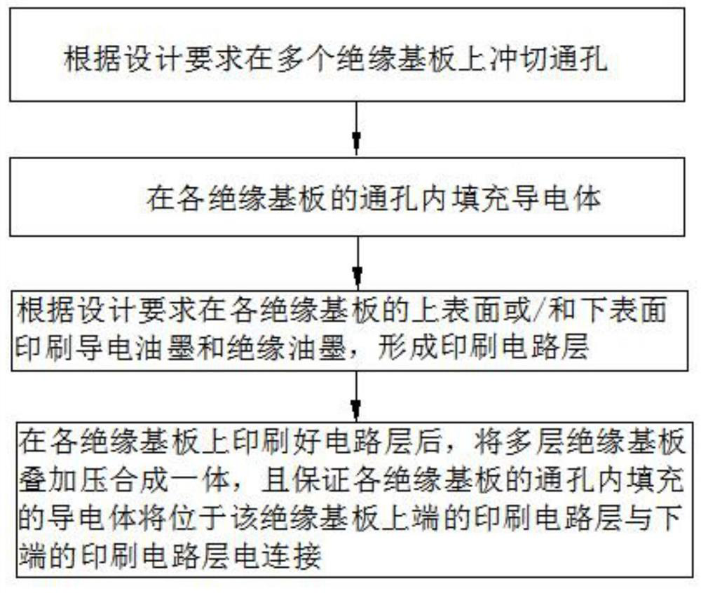
[0029] see Figure 1 to Figure 3 , an embodiment of the present invention provides a method for manufacturing a multilayer circuit board, comprising the following steps:

[0030] Punching through holes on multiple insulating substrates 1 according to design requirements;

[0031] Filling conductors 3 in the through holes of each insulating substrate 1;

[0032] Print conductive ink and insulating ink on the upper surface or / and lower surface of each insulating substrate 1 according to design requirements to form a printed circuit layer 2;

[0033] After the circuit layer is printed on each insulating substrate 1, the multi-layer insulating substrate 1 is superimposed and pressed into one body, and it is ensured that the conductor 3 filled in the through hole of each insulating substrate will be located at the printed circuit layer at the upper end of the insulating substrate and the printed circuit layer at the lower end. The printed circuit layers are electrically connected...

Embodiment 2

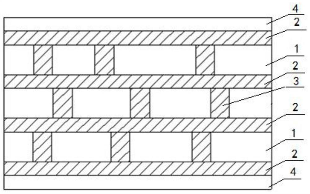
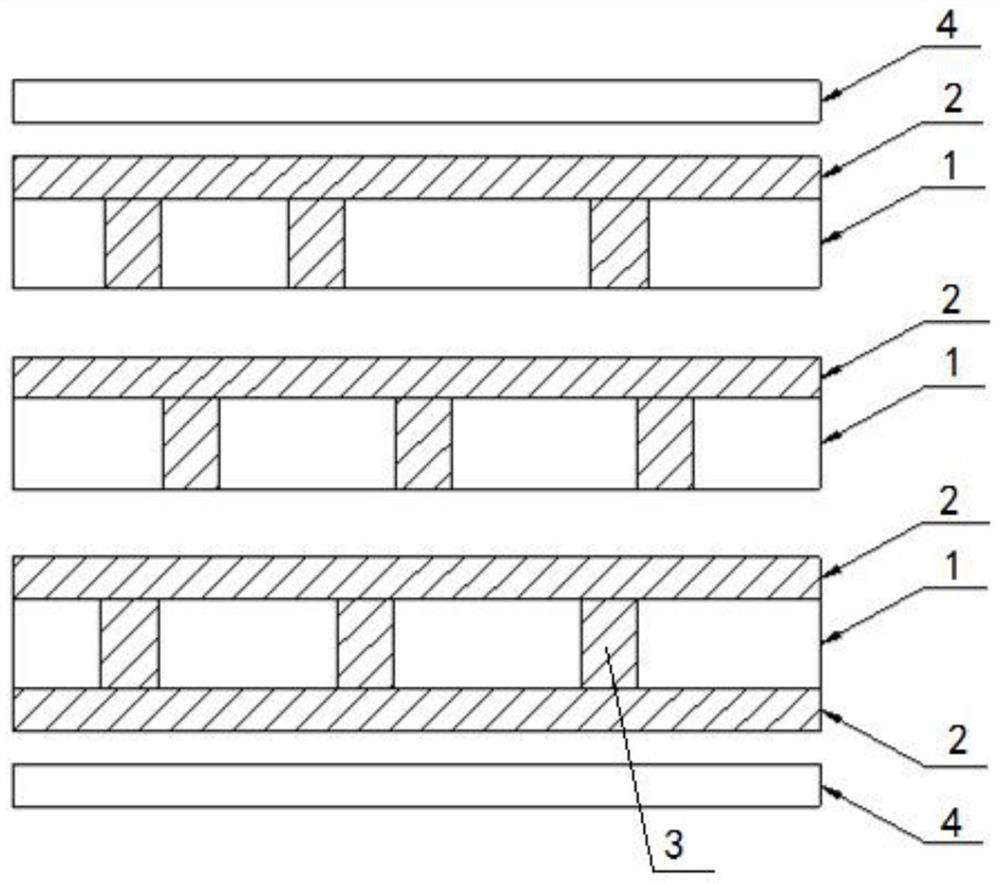
[0040] see figure 2 and image 3 , the embodiment of the present invention provides a multilayer circuit board, including a multilayer insulating substrate 1 (that is, two or more layers), the upper surface or / and lower surface of the insulating substrate 1 is printed with conductive ink and insulating ink, The printed circuit layer 2 is formed, and the multi-layer insulating substrates 1 are superimposed and pressed together, and each layer of insulating substrates 1 is provided with through holes, and the through holes are filled with conductors 3 for printing on the upper end of the insulating substrate 1. The circuit layer 2 is electrically connected to the printed circuit layer 2 at the lower end.

[0041] Further, the material of the insulating substrate 1 is an insulating resin substrate.

[0042] Further, only one printed circuit layer 2 is provided between each insulating substrate 1 .

[0043] Further, a circuit layer is printed on the upper surface of the upperm...


PUM


Abstract

The invention relates to a multilayer circuit board manufacturing method and a multilayer circuit board. The method comprises the following steps: punching through holes in a plurality of insulating substrates according to design requirements; filling conductors in the through holes of the insulating substrates; printing conductive ink and insulating ink on the upper surface or / and the lower surface of each insulating substrate according to design requirements to form a printed circuit layer; and after the circuit layers are printed on the insulating substrates, stacking and pressing the multiple layers of insulating substrates into a whole to guarantee that the printed circuit layer located at the upper end of the insulating substrate is electrically connected with the printed circuit layer located at the lower end of the insulating substrate through the electric conductors filled in the through holes of the insulating substrates. Circuit characteristics are achieved through the conductive ink and the insulating ink, an original high-energy-consumption and high-pollution base material is replaced with an environment-friendly material, the conductive performance is achieved through a traditional printing technology, circuit opening and closing are achieved through a traditional punching infiltration mode, and through the traditional printing technology and multi-layer lamination pressurization synthesis forming, the operation process is reduced, and the production efficiency is improved, so the manufacturing cost is reduced, and environmental protection is achieved.

Description

technical field [0001] The invention belongs to the technical field of circuit board production, and in particular relates to a multilayer circuit board production method and the multilayer circuit board. Background technique [0002] The manufacturing process of conventional multilayer printed circuit boards generally includes the following processes: material cutting-inner drawing (including film, exposure and development)-inner etching-adhesion pressing-drilling-copper sinking-electroplating-outer drawing (including Film, exposure and development) - external etching - external inspection - solder mask - exposure - characters - surface coating - appearance - electrical testing - final review - final inspection - packaging. [0003] The process of the above-mentioned process is complicated and time-consuming, and it usually takes many days to finally produce the required circuit board. Moreover, the above process adopts copper foil blanking to process the circuit pattern, ...

Claims


Application Information

Patent Timeline
Patent Type & Authority Applications(China)
IPC IPC(8): H05K3/46H05K3/00
CPCH05K3/4614H05K3/4626H05K3/005
Inventor 钱大伟
Owner WUHAN TIANYU INFORMATION IND
Why Eureka
Try Eureka