Preparation method of packaging substrate circuit

A technology for packaging substrates and circuits, applied in multilayer circuit manufacturing, printed circuit manufacturing, printed circuits, etc., can solve problems affecting electrical quality, poor bonding, small area, etc., and achieve good uniformity, good bonding, and increased The effect of subsequent area

Pending Publication Date: 2022-02-01
苏州群策科技有限公司
View PDF0 Cites 0 Cited by
  • Summary
  • Abstract
  • Description
  • Claims
  • Application Information

AI Technical Summary

Problems solved by technology

[0002] As the circuit board circuit continues to develop towards finer circuit precision, the circuit formed on the circuit board is thinner and the gap between the lines is narrower. Therefore, when the circuit layer is subsequently added to the circuit layer, the dielectric layer is not easy to fill the circuit. The gap between them is easy to have air bubbles remaining in it, which seriously affects the reliability of the formed circuit board
And because the line width of the thin line is thinner, the bonding area between the bottom and the dielectric layer is smaller, and there is a problem of poor bonding
And because the conductive layer is used as the current conduction path during electroplating, the current density flowing through different parts of the conductive layer is different, resulting in uneven thickness of the circuit layer formed by electroplating metal on the conductive layer, which affects the smoothness of the surface of the circuit layer, and then affects the electric current. sexual quality

Method used


Image

  • Preparation method of packaging substrate circuit
  • Preparation method of packaging substrate circuit
  • Preparation method of packaging substrate circuit

Examples


Embodiment 1

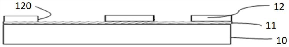
[0050] combine Figure 1A to Figure 1H , the preparation method of the packaging substrate circuit, comprising the following steps:

[0051] First, the worker provides a circuit board. The surface of the circuit board is provided with a conductive copper layer.

[0052]Secondly, a first dielectric layer is formed on the surface of the conductive copper layer. The material of the first dielectric layer can be photosensitive or non-photosensitive material, specifically, it can be ABF (Ajinomotobuild-up film), epoxy resin (Epoxy resin), polyimide (Polyimide), cyanate ester (Cyanate Ester), Glass fiber, bismaleimide triazine (Bismaleimide Triazine, BT) or FR5 material mixed with epoxy resin and glass fiber. And a first opening is opened in the first dielectric layer to expose part of the surface of the conductive copper layer. The first opening is formed by laser drilling or exposure and development.

[0053] Secondly, a conductive circuit is formed in the first opening by che...

Embodiment 2

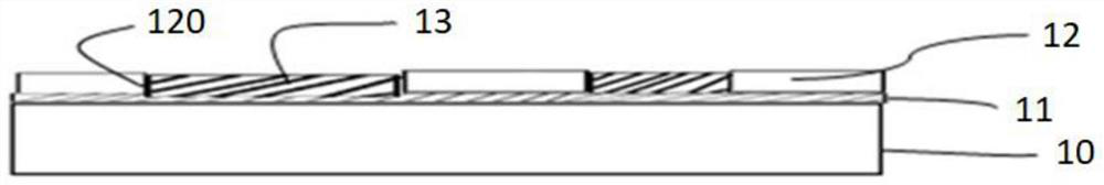
[0059] combine Figure 1A to Figure 1D , Figure 2A to Figure 2D , the preparation method of the packaging substrate circuit, comprising the following steps:

[0060] First, the worker provides a circuit board. The surface of the circuit board is provided with a conductive copper layer.

[0061] Secondly, a first dielectric layer is formed on the surface of the conductive copper layer. The material of the first dielectric layer can be photosensitive or non-photosensitive material, specifically, it can be ABF (Ajinomotobuild-up film), epoxy resin (Epoxy resin), polyimide (Polyimide), cyanate ester (Cyanate Ester), Glass fiber, bismaleimide triazine (Bismaleimide Triazine, BT) or FR5 material mixed with epoxy resin and glass fiber. And a first opening is opened in the first dielectric layer to expose part of the surface of the conductive copper layer. The first opening is formed by laser drilling or exposure and development.

[0062] Secondly, a conductive circuit is forme...

Embodiment 3

[0068] combine Figure 1A to Figure 1D , Figure 3A to Figure 3D , the preparation method of the packaging substrate circuit, comprising the following steps:

[0069] First, the worker provides a circuit board. The surface of the circuit board is provided with a conductive copper layer.

[0070] Secondly, a first dielectric layer is formed on the surface of the conductive copper layer. The material of the first dielectric layer can be photosensitive or non-photosensitive material, specifically, it can be ABF (Ajinomotobuild-up film), epoxy resin (Epoxy resin), polyimide (Polyimide), cyanate ester (Cyanate Ester), Glass fiber, bismaleimide triazine (Bismaleimide Triazine, BT) or FR5 material mixed with epoxy resin and glass fiber. And a first opening is opened in the first dielectric layer to expose part of the surface of the conductive copper layer. The first opening is formed by laser drilling or exposure and development.

[0071] Secondly, a conductive circuit is forme...


PUM


Abstract

The invention discloses a preparation method of a packaging substrate circuit, which comprises the following steps of: providing a circuit board, and arranging a conductive copper layer on the surface of the circuit board; forming a first dielectric layer on the surface of the conductive copper layer, and forming a first opening in the first dielectric layer; forming a conductive circuit in the first opening in a chemical deposition mode; removing the first dielectric layer and the conductive copper layer covered by the first dielectric layer to form a circuit covering the surface of the circuit board; forming a second dielectric layer on the surface of the circuit board; forming a third dielectric layer on the surface of the second dielectric layer, and forming a second opening and a third opening in the third dielectric layer at an interval; and forming a chemical plating metal line layer in the second opening and the third opening. The multi-layer plated metal is formed in the first dielectric layer in a chemical deposition mode to form the multi-layer plated metal circuit layer, the bonding area of the multi-layer plated metal circuit layer and the first dielectric layer is increased, the bonding force between the second dielectric layer and the circuit structure is better, and the uniformity of the thickness of the circuit structure is better.

Description

technical field [0001] The invention relates to the technical field of PCB boards, in particular to a method for preparing a packaging substrate circuit. Background technique [0002] As the circuit board circuit continues to develop towards finer circuit precision, the circuit formed on the circuit board is thinner and the gap between the lines is narrower. Therefore, when the circuit layer is subsequently added to the circuit layer, the dielectric layer is not easy to fill the circuit. Air bubbles are likely to remain in the gap between them, which seriously affects the reliability of the formed circuit board. Moreover, since the line width of the thin line is thinner, the bonding area between the bottom of the thin line and the dielectric layer is smaller, and there is a problem of poor bonding. And because the conductive layer is used as the current conduction path during electroplating, the current density flowing through different parts of the conductive layer is diff...

Claims


Application Information

Patent Timeline
IPC IPC(8): H05K3/46
CPCH05K3/4661
Inventor 王晓超
Owner 苏州群策科技有限公司
Why Eureka
Try Eureka