Negative capacitance junction-free nanowire field effect transistor and manufacturing method thereof
A technology for field effect transistors and manufacturing methods, applied in semiconductor/solid-state device manufacturing, circuits, electrical components, etc., can solve the problems of electrical performance to be improved, small on-state current, and slow turn-on speed, and achieve electrical performance improvement and drive Effect of large current and reduced power consumption
- Summary
- Abstract
- Description
- Claims
- Application Information
AI Technical Summary
Problems solved by technology
Method used
Image

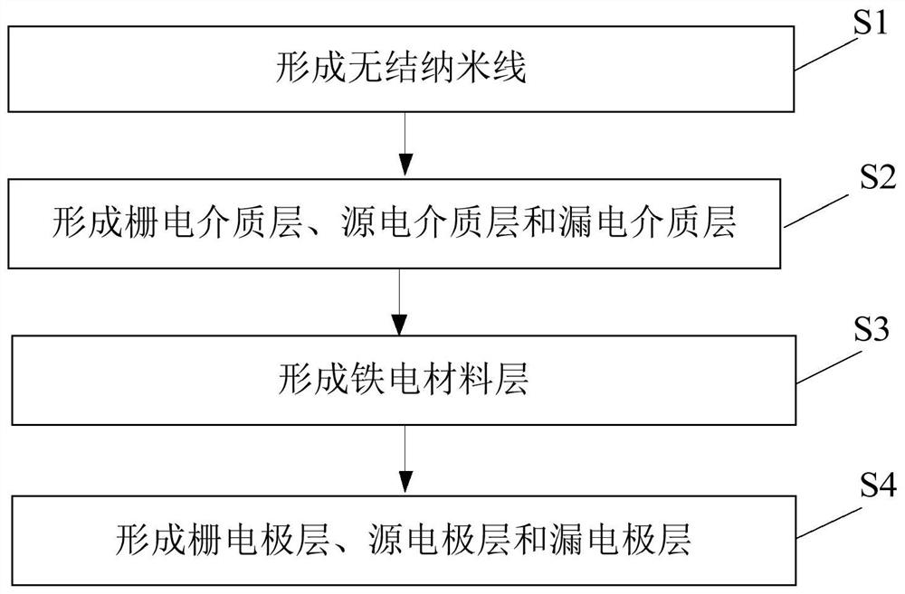
Examples
Embodiment 1
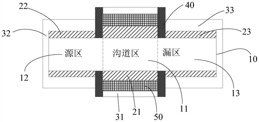
[0052] figure 1 A negative capacitance non-knotted nanowire field effect transistor structure provided by the present embodiment, figure 1 The non-knotted nanowire field effect transistor includes: a non-knotted nanowire 10 including a source region 12, a channel region 11, and a drain region 13 defined in the axial direction thereof.
[0053] In the present embodiment, the non-knotted nanowire 10 is a single crystal silicon column having both ends of the cylinder, respectively, from the void region 13, and is the channel region 11 ( figure 1 For section, the non-knotted nanowire 10 can also be understood as a strip-like single crystal silicon rod body of the transistor on the SOI substrate, including the source region 12, a channel region 11 and a drain region. 13. Wherein, the source region 12, the channel region 11, and the drain region 13 are axisymmonic.
[0054] It should be noted that the single crystal silicon rod can be doped or lightly doped, and when it is lightly dope...
Embodiment 2
[0090] Example embodiments of the present embodiment differs from the embodiment only in that a field effect transistor without the nanowire junction source and drain regions having the same doping type as the channel region of the doped region and the source region and doped drain region is heavily doped region, the channel region is a lightly doped region. Hereinafter, the embodiment of the present embodiment in conjunction with the accompanying drawings, the detailed description of the distinction portion further, the article to avoid redundancy, a repeat portion of the embodiment will be omitted.
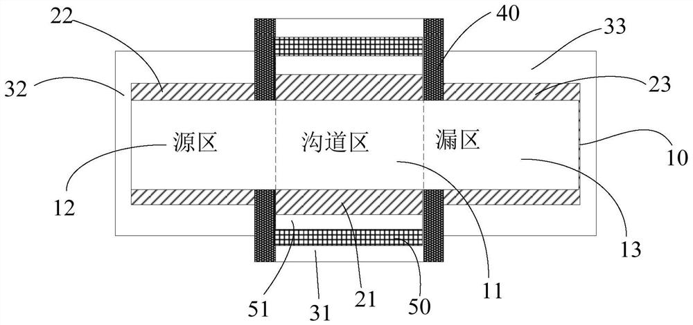
[0091] Figure 10 Knotless schematic structure of a nanowire field effect transistor provided in the present embodiment, with reference to Figure 10 The knotless nanowire field effect transistor comprising: None nanowire junction 100, junction 100 without the source region along the axial direction of the nanowire 101 are sequentially defined, the channel region 103 and drain region...
PUM
| Property | Measurement | Unit |
|---|---|---|
| thickness | aaaaa | aaaaa |
| electron work function | aaaaa | aaaaa |
| electron work function | aaaaa | aaaaa |
Abstract
Description
Claims
Application Information