Flexible stretchable gold film electrode based on reactive ion etching and preparation method thereof
A reactive ion etching, flexible technology, applied in the direction of ion implantation plating, metal material coating process, coating, etc., can solve unfavorable wearable biological signal monitoring, flexible electrode stability is not high, stretchability Insufficient and high problems, to achieve the effect of excellent stretchability, excellent interfacial adhesion, and few steps
- Summary
- Abstract
- Description
- Claims
- Application Information
AI Technical Summary
Problems solved by technology
Method used
Image
Examples
preparation example Construction
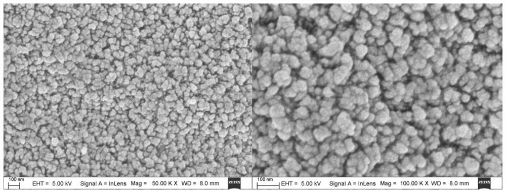
[0030] A method for preparing a highly stretchable flexible gold film electrode comprises the following steps: magnetron sputtering a layer of gold film 3 on the surface of a polymer flexible substrate treated by a reactive ion etching process. The thickness of the gold thin film 3 is 10-40 nanometers, and the gold thin film 3 has a micron and / or nanoscale crack structure.
[0031] In this application, the reactive ion etching method is used to process the surface of the polymer substrate to change its surface properties and microscopic morphology, thereby affecting the performance of the gold film 3 deposited by magnetron sputtering. The gold film 3 deposited on it has microns and Nanoscale crack structure. Since the gold film 3 produces micro- and nano-scale crack structures during the magnetron sputtering deposition process, when the gold film 3 is subjected to tensile stress, the micro-cracks can undergo surface deformation, so that a large external force stretches only on...
Embodiment 1
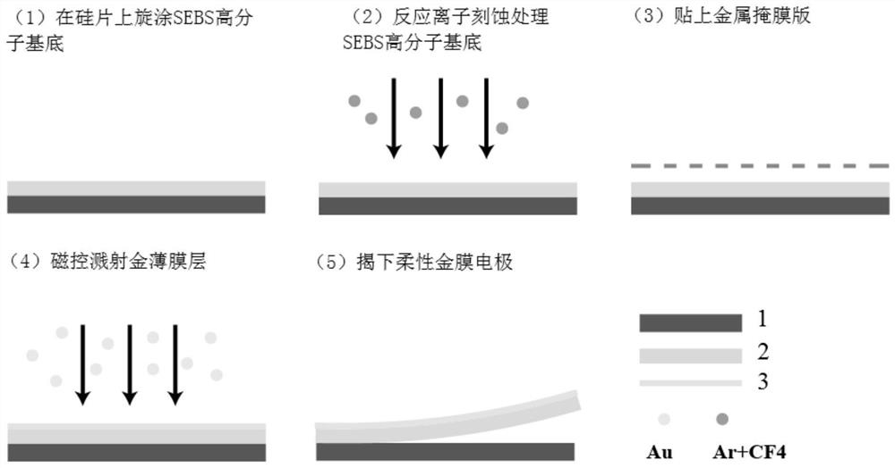
[0044] Embodiment 1: refer to figure 1 , the embodiment of the present application provides a method for preparing a highly stretchable flexible gold film electrode, comprising the following steps:
[0045] Step 1: Dissolving SEBS particles in dimethylformamide solvent to prepare a 15% concentration solution, spin-coating on a three-inch silicon wafer 1, and standing for 10 hours until SEBS volatilizes to form a film to obtain SEBS polymer substrate 2;
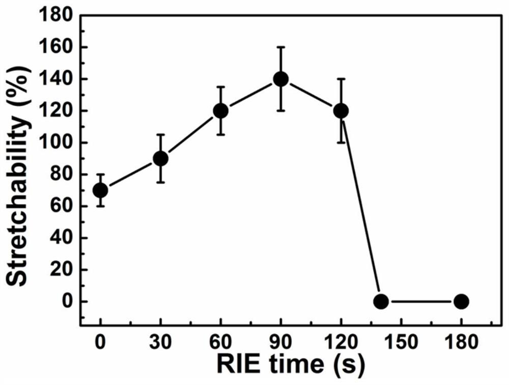
[0046] Step 2: Put the SEBS polymer substrate 2 in the reactive ion etching equipment, adjust the parameters of Ar gas 10ccm, CF4 gas 30ccm, 13.3Pa, 150W, etch for 90 seconds;
[0047] Step 3: Paste the patterned metal mask on the surface of the SEBS polymer flexible substrate in step 2, and absorb it with a magnet to make it tightly attached;
[0048] Step 4: Magnetron sputtering a layer of gold film 3 on the surface of the SEBS polymer flexible substrate, the thickness of the gold film 3 is 20 nanometers, the process is a s...
PUM
| Property | Measurement | Unit |
|---|---|---|
| thickness | aaaaa | aaaaa |
| thickness | aaaaa | aaaaa |
Abstract
Description
Claims
Application Information


