Nanoporous semiconductor thin films

a semiconductor and thin film technology, applied in the field of nanoporous semiconductor thin films, can solve the problems of low sensing performance of ofet-based chemical sensors, low sensitivity, and low precision, and achieve the effects of improving sensitivity, excellent performance, and improving sensitivity

Active Publication Date: 2018-02-22
THE BOARD OF TRUSTEES OF THE UNIV OF ILLINOIS
View PDF1 Cites 19 Cited by
  • Summary
  • Abstract
  • Description
  • Claims
  • Application Information

AI Technical Summary

Benefits of technology

[0006]Templated by a nanostructured layer of poly(4-vinylphenol) (PVP) and 4,4′-(hexafluoroisopropylidene)diphthalic anhydride (HDA), the pore sizes in a semiconductor layer were widely tunable from 50 nm to 1 μm. Thus, introducing nanopores to OFET sensors enhances its reactivity towards VOCs such as ammonia by an order of magnitude, revealed by the reaction model established herein. As a result, the nanopores enabled ultrasensitive, ultrafast response to ammonia down to 1 ppb at hundred-millisecond time scale, which is the best sensing performance reported so far. The generality this strategy was further demonstrated by fabricating nanoporous small molecules for formaldehyde sensing. A 10-fold sensitivity enhancement with unprecedented sensitivity down to 1 ppb was obtained, which is three orders of magnitude better than previous OFET formaldehyde sensors. The excellent performance, simple fabrication, diverse form-factors of nanoporous transistors opens up a wide range of applications in personalized health and environmental monitoring, frequently demanding sensitivity on the ppb level with fast response. The disclosed approach of printing nanoporous thin films could be extended to other material systems and various solution processing methods. Furthermore, the concept of nanoporous organic electronics can bring novel properties beyond chemical sensitivity, such as enhanced mechanical stretchability, new optical properties, and even application in controlled drug release.
[0007]Additionally, introducing the porous structure into the organic semiconductors contributes to the doping process after adding the dopant layer in the film device. Given the impact of the pore size and dopant selectivity, the host organic semiconductor could be switched between n- and p-channel with a doping process by fine-tuning the pore structure. Hence, pore structure in the active layer also opens opportunities for modulating the transport of a unipolar material by an effective doping process between p-type, ambipolar and n-type semiconductors. The enhanced-doping properties also benefit to the increase of the carrier mobility as well as film conductivity, which show a bright future in organic electronics, such as field-effect transistors and thermoelectrics.

Problems solved by technology

Reported sensing performances of OFET-based chemical sensors frequently fall short of the high requirements for realizing personalized health and environmental monitoring via detection of volatile organic compounds (VOCs).
The response time is also non-ideal, ranging from seconds to minutes.
Due to the stringent requirement on detection limit, VOC detection and analysis still rely on complex, bulky spectroscopic methods, which are not available to common household.

Method used


Image

  • Nanoporous semiconductor thin films
  • Nanoporous semiconductor thin films
  • Nanoporous semiconductor thin films

Examples


example 1

Templating Nanoporous OSC Thin Films

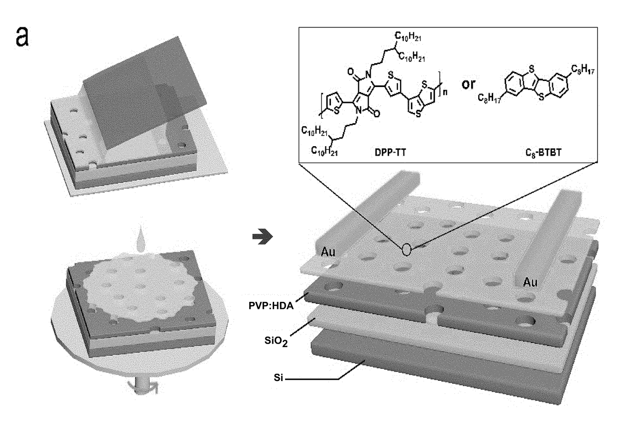
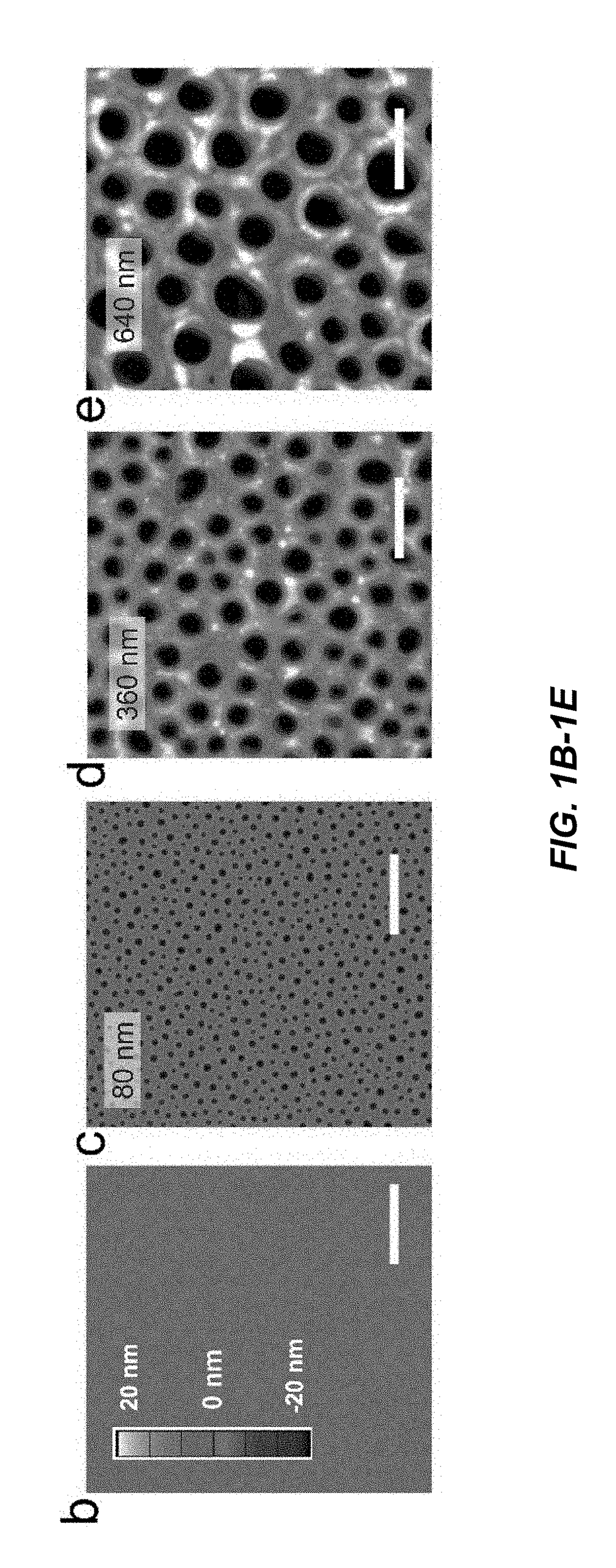
[0152]We demonstrate a simple, additive approach to fabricate nanoporous semiconductor thin films in solution processing. The solution processing methods we used include spin coating and meniscus-guided unidirectional coating; the latter shares the same fundamental physics as large-scale roll-to-roll printing (FIG. 1a). The simplicity and generality of this approach for fabricating nanoporous thin films stand in contrast to the conventional subtractive approaches based on lithography and etching, which involve complex procedures and corrosive chemicals. The key to our method is to direct the semiconductor deposition using a nanoporous insulating layer serving as the template, which can be fabricated over a large area via one-step microphase separation during spin coating. The nanoporous template was prepared from poly(4-vinylphenol) (PVP) / tetrahydrofuran (THF) solution with 4,4′-(Hexafluoroisopropylidene) diphthalic anhydride (HDA) added as the cr...

example 2

Characterization of Nanoporous Semiconductor Films

[0154]We further characterized the molecular packing in the nanoporous semiconductor films by Grazing-incidence X-ray diffraction (GIXD) (FIG. 2d-f, FIGS. 9 and 10). The detailed molecular packing analysis is summarized in Table 3 and Table 4. Not surprisingly, the presence of nanopores did not noticeably alter the molecular packing in the DPP-TT thin film.

[0155]FIG. 2g shows the geometrically corrected orientation distribution of crystallites in coated DPP-TT films obtained from pole-figure analysis on the π-π stacking ring. The analysis unveiled a predominant edge-on orientation of the 7C stacks (FIG. 2h and FIG. 9g) in all cases tested regardless of the processing methods and the pore sizes. We expect this preferred orientation to promote the charge-transfer reaction with the analyte by maximizing the exposure of the π orbitals of the conjugated core at the pore wall.

[0156]How does the nanoporous template direct the semiconductor ...

example 3

Nanoporous Polymer OFET for Ammonia Sensing

[0157]To characterize the charge transport properties and sensing performance of the nanoporous semiconductor thin films, we fabricated top contact bottom gate transistor devices and performed electrical measurements under ambient conditions (FIG. 3). Typical transfer curves of DPP-TT OFETs with and without pores are shown in FIG. 3a. Both devices exhibited predominant hole transport with an on / off ratio of ˜105. The DPP-TT based nanoporous OFETs had comparable mobility (0.30±0.05 cm2V−1s−1) but slightly lower on-current compared to the nonporous devices, due to a slight decrease in capacitance when the nanostructured template layer was introduced (FIG. 14). This observation confirms that introducing nanopores did not adversely influence the device performance. Notably, the transistor devices remained stable after repeated measurements in air, which is ideal for sensing applications (FIG. 15).

[0158]We next measured the sensing performance o...


PUM

PropertyMeasurementUnit
pore diameteraaaaaaaaaa
pore sizesaaaaaaaaaa
widthaaaaaaaaaa

Abstract

The present disclosure provides a method of fabricating a nanoporous thin film device comprising depositing a template on a substrate to form a nanoporous insulating layer, the template comprising one or more polymers capable of forming pores when polymerized and at least one cross-linking agent, and depositing a second layer (e.g. organic semiconductor, semiconductor, insulator) on the nanopourous insulating layer to form a thin film having a plurality of isolated nanopores on the surface. Nanoporous semiconductor thin films made by these methods is provided. Sensors and devices comprising the nanoporous thin film is also disclosed.

Description

RELATED APPLICATIONS[0001]This application claims priority under 35 U.S.C. § 119(e) to U.S. Provisional Patent Application No. 62 / 375,475, filed Aug. 16, 2016, which is incorporated herein by reference.BACKGROUND OF THE INVENTION[0002]Organic semiconductors (OSC) have emerged as a new class of electronic materials promising a wide range of applications from organic field-effect transistors (OFET), solar cells, thermoelectrics, electronic skins, chemical and mechanical sensors by virtue of their chemical versatility, solution processability and mechanical flexibility. OFET-based chemical sensing presents a combination of advantages including field-effect enabled signal amplification, tunable selectivity and sensitivity by accessing vast chemical and morphological design spaces, as well as solution printability for manufacturing massively deployable low-cost sensor chips which are expected to power the Internet of Things in a foreseeable future.[0003]Reported sensing performances of O...

Claims


Application Information

Patent Timeline
Patent Type & Authority Applications(United States)
IPC IPC(8): G01N27/414H01L51/05H01L51/00G01N33/00G01N33/497
CPCG01N27/4141G01N2033/4975H01L51/0096H01L51/0014H01L51/0533G01N27/4146G01N33/0054G01N33/0047G01N33/497H01L51/004H01L51/0036H01L51/0074H01L51/0071H01L51/0558H01L51/0545Y02E10/549Y02A50/20H10K85/111H10K85/113H10K85/151H10K85/6576H10K10/476H10K10/486H10K10/466H10K71/20H10K77/10H10K85/141H10K85/657H10K10/484
Inventor DIAO, YINGZHANG, FENGJIAO
Owner THE BOARD OF TRUSTEES OF THE UNIV OF ILLINOIS
Why Eureka
Try Eureka