
Short-channel field effect transistor and manufacturing method thereof

A manufacturing method and technology for effect transistors, which are applied in semiconductor/solid-state device manufacturing, electrical components, circuits, etc., can solve the problems of complex control operation process and low precision of channel length control, and achieve simple, stable and easy-to-implement operation process. Effect

Pending Publication Date: 2022-03-01
ZHUZHOU CRRC TIMES SEMICON CO LTD
View PDF0 Cites 0 Cited by
  • Summary
  • Abstract
  • Description
  • Claims
  • Application Information

AI Technical Summary

Problems solved by technology

[0004] In view of this, the purpose of one or more embodiments of this specification is to propose a short channel field effect transistor and its manufacturing method to solve the problems of low channel length control accuracy and complicated control operation process in field effect transistor production

Method used


Image

  • Short-channel field effect transistor and manufacturing method thereof
  • Short-channel field effect transistor and manufacturing method thereof
  • Short-channel field effect transistor and manufacturing method thereof

Examples


Embodiment Construction

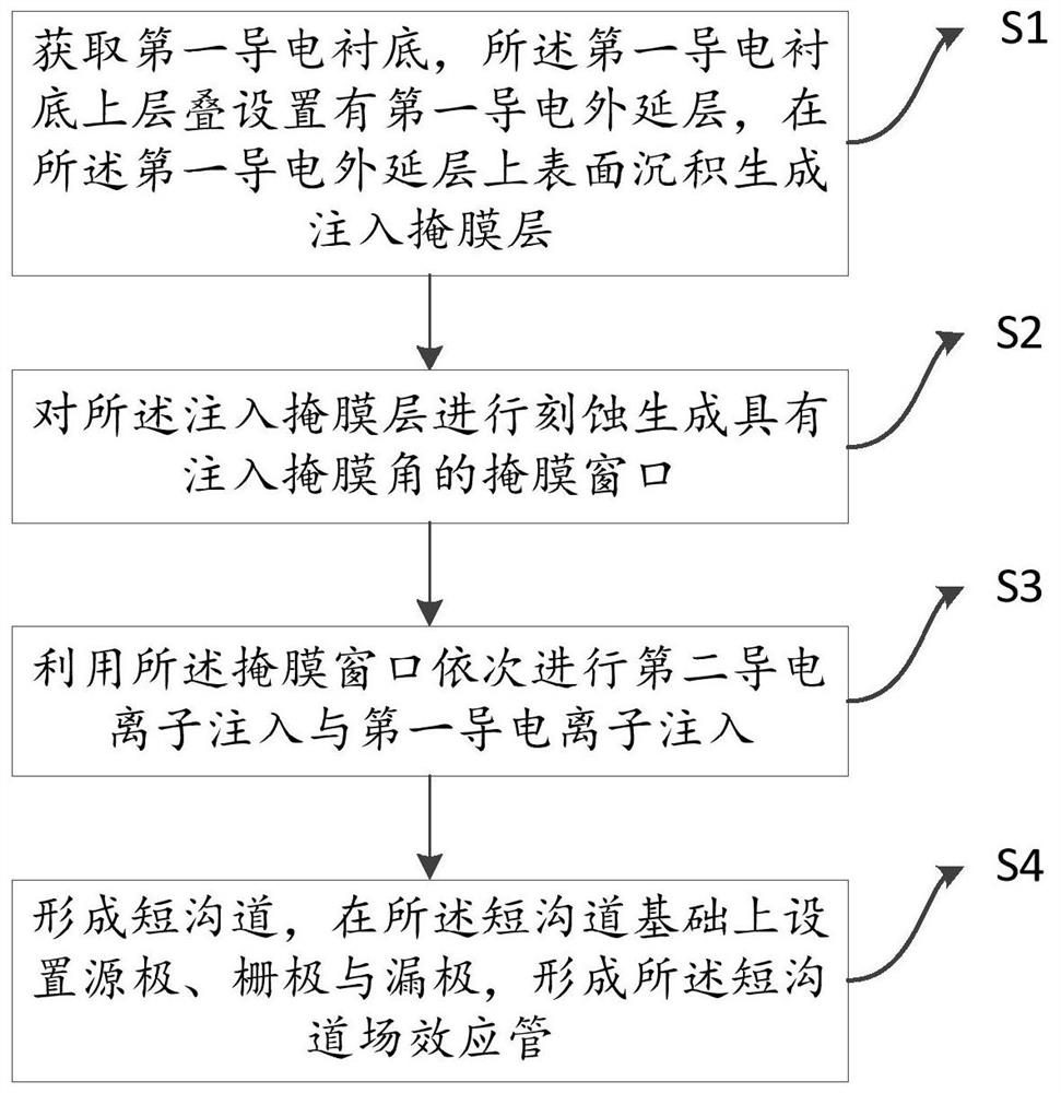
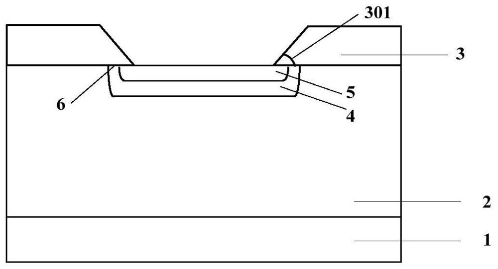
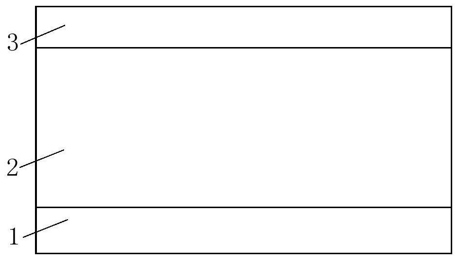
[0055] In order to make the purpose, technical solutions and advantages of the present disclosure clearer, the present disclosure will be further described in detail below in conjunction with specific embodiments and with reference to the accompanying drawings.

[0056] It should be noted that, unless otherwise defined, the technical terms or scientific terms used in one or more embodiments of the present specification shall have the common meanings understood by those skilled in the art to which the present disclosure belongs. "First", "second" and similar words used in one or more embodiments of this specification do not indicate any order, quantity or importance, but are used to distinguish different components. "Comprising" or "comprising" and similar words mean that the elements or items appearing before the word include the elements or items listed after the word and their equivalents, and do not exclude other elements or items. "Connected" or "connected" and similar terms...


PUM

PropertyMeasurementUnit
Thicknessaaaaaaaaaa

Abstract

One or more embodiments of the invention provide a short-channel field effect transistor and a manufacturing method thereof. The short-channel field effect transistor can accurately control the channel length and is simple in control operation process. The method comprises the following steps: acquiring a first conductive substrate and a first conductive epitaxial layer, and depositing and generating an injection mask layer on the upper surface of the first conductive epitaxial layer; etching the injection mask layer to generate a mask window with an injection mask angle; second conductive ion implantation and first conductive ion implantation are sequentially carried out through the mask window, wherein the second conductive ions are vertically implanted, and the first conductive ions are symmetrically and obliquely implanted; a short channel is formed in the part, exceeding the first conductive doped region, of the second conductive doped region, and a source electrode, a grid electrode and a drain electrode are arranged on the basis of the short channel, so that the short-channel field effect transistor is formed. The short-channel field effect transistor is manufactured by using the manufacturing method.

Description

technical field [0001] One or more embodiments of this specification relate to the technical field of semiconductor device fabrication, and in particular to a short channel field effect transistor and a fabrication method thereof. Background technique [0002] Silicon carbide metal oxide semiconductor field effect transistor (SiC MOSFET) has the characteristics of low on-resistance, fast switching speed, high temperature resistance, etc., and has great application advantages in high-voltage frequency conversion, new energy vehicles, rail transit and other fields. In order to increase the current density of MOSFET, effectively controlling and shortening the channel length of the device has become one of the main research directions. [0003] In the existing methods of controlling and shortening the channel length of SiC MOSFET, the sidewall after polysilicon oxidation is mostly used as the injection barrier layer to control the channel. The area range of the conductive doped ...

Claims


Application Information

Patent Timeline
IPC IPC(8): H01L21/04H01L29/78
CPCH01L21/0445H01L21/0465H01L21/047H01L29/66068H01L29/78
Inventor 罗烨辉郑昌伟焦莎莎丁杰钦王志成刘芹王亚飞李诚瞻
Owner ZHUZHOU CRRC TIMES SEMICON CO LTD
Features
  • Generate Ideas
  • Intellectual Property
  • Life Sciences
  • Materials
  • Tech Scout
  • Unparalleled Data Quality
  • Higher Quality Content
  • 60% Fewer Hallucinations
Learn More