
Eureka
For R&D, Eureka makes reading and utilizing patents & technical documents easy.
Eureka AIR
Designed for self-driven R&D workflows. Generate viable solutions, solve complex R&D challenges, empower your innovation with AI.

Eureka Materials
Designed for material experts only. Revolutionize your material R&D, from search, analyze, to developing new materials.

TechResearch
Generate reliable direction feasibility study reports for your R&D in just a few steps.

TechSeek
Discover and master advanced knowledge NOW. Basics, ideas, possibilities, all at once.

TechMind
As an expert in R&D Theories, TechMind can generates customized viable solutions instantly.

TechRisk
Analyze your overall solution with one click, know your potential R&D risks in advance.

TechMonitor
Get weekly tech updates, stay abreast of the latest tech innovations and key insights.
Semiconductor structure and forming method thereof
A semiconductor and conductive layer technology, applied in the fields of semiconductor devices, semiconductor/solid-state device manufacturing, semiconductor/solid-state device components, etc., can solve the problems of poor performance of metal interconnect structures, and achieve improved performance, lower resistance, and lower contact resistance. Effect
- Summary
- Abstract
- Description
- Claims
- Application Information
AI Technical Summary
Problems solved by technology
Method used
Image

Examples
Embodiment Construction
[0041] It should be noted that the "surface" and "upper" in this specification are used to describe the relative positional relationship in space, and are not limited to direct contact.
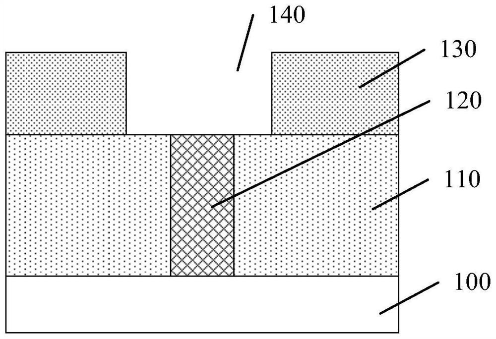
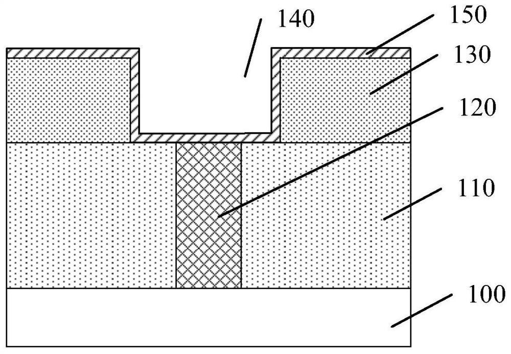
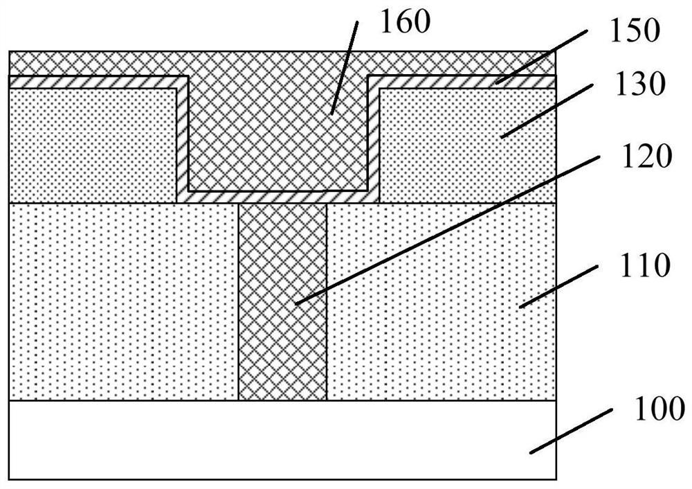
[0042] First, the reasons for the poor performance of existing semiconductor structures are described in detail in conjunction with the accompanying drawings, figure 1 to Figure 4 It is a structural schematic diagram of each step of a method for forming a conventional semiconductor structure.
[0043] Please refer to figure 1 , providing a substrate 100, the substrate 100 has a first dielectric layer 110, the first dielectric layer 110 has a first conductive layer 120 inside, and the first dielectric layer 110 exposes the top of the first conductive layer 120; Form the second dielectric layer 130 and the opening 140 in the second dielectric layer 130 on the surface of the first conductive layer 120 and the first dielectric layer 110, and the opening 140 exposes the top surface of the firs...
PUM
| Property | Measurement | Unit |
|---|---|---|
| thickness | aaaaa | aaaaa |
| thickness | aaaaa | aaaaa |
Abstract
Description
Claims
Application Information
 - R&D Engineer
- R&D Manager
- IP Professional
- Industry Leading Data Capabilities
- Powerful AI technology
- Patent DNA Extraction
Browse by: Latest US Patents, China's latest patents, Technical Efficacy Thesaurus, Application Domain, Technology Topic, Popular Technical Reports.
© 2024 PatSnap. All rights reserved.Legal|Privacy policy|Modern Slavery Act Transparency Statement|Sitemap|About US| Contact US: help@patsnap.com