Method of forming semiconductor device

A semiconductor and device technology, applied in the field of semiconductor device formation, can solve problems such as complex steps of fork-shaped nanosheet devices and influence on transistor characteristics, and achieve the effects of reducing photolithography steps, reducing critical dimensions and deviations, and reducing costs

Active Publication Date: 2022-05-10
GUANGZHOU CANSEMI TECH INC
View PDF3 Cites 0 Cited by
  • Summary
  • Abstract
  • Description
  • Claims
  • Application Information

AI Technical Summary

Problems solved by technology

[0005] The purpose of the present invention is to provide a method for forming a semiconductor device to solve the problem of complex steps of fork-shaped nanosheet devices and the influence of critical dimensions and deviation changes on transistor characteristics

Method used


Image

  • Method of forming semiconductor device
  • Method of forming semiconductor device
  • Method of forming semiconductor device

Examples


Embodiment Construction

[0062] A method for forming a semiconductor device proposed by the present invention will be further described in detail below with reference to the accompanying drawings and specific embodiments. Advantages and features of the present invention will be apparent from the following description and claims. It should be noted that all the drawings are in a very simplified form and use imprecise scales, and are only used to facilitate and clearly assist the purpose of illustrating the embodiments of the present invention.

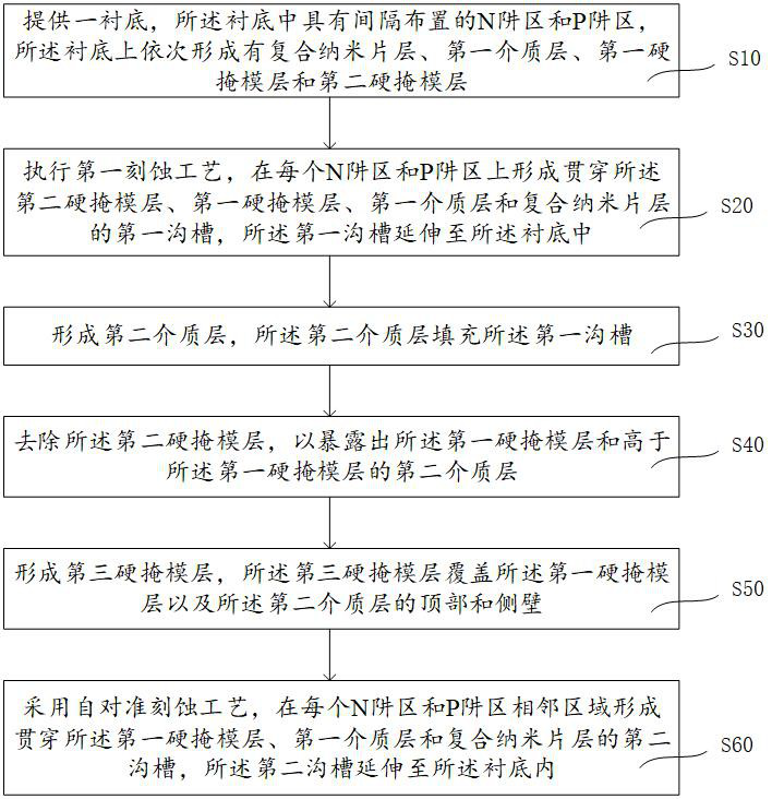
[0063] Specifically, please refer to figure 1 , which is a flowchart of a method for forming a semiconductor device according to an embodiment of the present invention. Such as figure 1 As shown, the present invention provides a method for forming a semiconductor device, comprising:

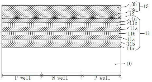
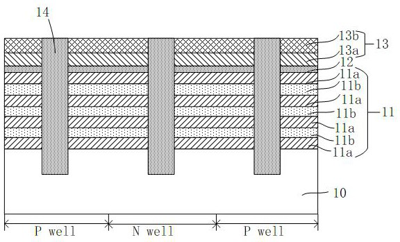
[0064] Step S10, providing a substrate, the substrate has N well regions and P well regions arranged at intervals, and the composite nanosheet layer, first dielectric layer, fi...


PUM

PropertyMeasurementUnit
thicknessaaaaaaaaaa
widthaaaaaaaaaa
thicknessaaaaaaaaaa

Abstract

The present invention provides a method for forming a semiconductor device, comprising: performing a first etching process, forming a second hard mask layer, a first hard mask layer, The first dielectric layer and the first groove of the composite nanosheet layer, the first groove extends into the substrate; a second dielectric layer is formed, and the second dielectric layer fills the first groove; removing The second hard mask layer to expose the first hard mask layer and the second dielectric layer higher than the first hard mask layer; forming a third hard mask layer, the third hard mask layer The mask layer covers the first hard mask layer and the top and sidewalls of the second dielectric layer; a self-aligned etching process is used to form through the adjacent regions of each N well region and P well region. The first hard mask layer, the first dielectric layer and the second groove of the composite nanosheet layer. A self-aligned etching process is adopted to reduce photolithography steps, reduce costs, and improve transistor performance.

Description

technical field [0001] The invention relates to the technical field of semiconductor manufacturing, in particular to a method for forming a semiconductor device. Background technique [0002] The Fin Field Effect Transistor (FinFET) architecture is the workhorse of today's semiconductor industry. However, as the device continues to shrink, when the channel length is small to a certain value, the fin field effect transistor structure cannot provide sufficient electrostatic control and sufficient driving current. Therefore, a nanosheet (Nanosheet) structure is introduced. Compared with fin field effect transistors, the characteristics of nanosheets provide excellent channel control capabilities, and at the same time, the excellent distribution of channels in three dimensions optimizes the effective drive current per unit area. [0003] As semiconductor device dimensions continue to shrink, further reductions in cell height will require smaller spacing between NMOS devices and...

Claims


Application Information

Patent Timeline
Patent Type & Authority Patents(China)
IPC IPC(8): H01L21/8238
CPCH01L21/823878H01L21/823821
Inventor 余自强
Owner GUANGZHOU CANSEMI TECH INC
Why Eureka
Try Eureka