
Manufacturing method of semiconductor device and PIN photodiode

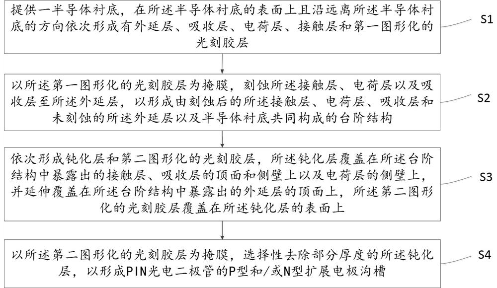
A manufacturing method and semiconductor technology, applied in the direction of semiconductor devices, circuits, electrical components, etc., can solve the problems of high cost, dielectric film separation, large stress, etc., and achieve the effect of improving device performance, reducing manufacturing costs, and reducing costs.

Pending Publication Date: 2022-03-18
浙江光特科技有限公司
View PDF6 Cites 0 Cited by
  • Summary
  • Abstract
  • Description
  • Claims
  • Application Information

AI Technical Summary

Problems solved by technology

[0003] For high-speed PIN photodetectors, there is a one-step process in its existing device manufacturing process that is the passivation process of the device. For example, the existing manufacturing processes such as 10GPIN, 25G PIN, and 36G PIN all use organic passivation film BCB (benzene And cyclobutene BCB) to replace the chemical vapor deposition passivation process to reduce the stress of the device, thereby reducing the junction capacitance, but due to the high cost of the organic passivation film BCB, and the main source of this material depends on imports, which in turn leads to photodetection The problem of high manufacturing cost of devices; for this problem, if the lower cost of inorganic passivation film (Si3N4 and SiO2) is used for passivation, although the manufacturing cost of photodetector devices can be reduced, the inorganic passivation film material will Introduce a large stress, and in the process of rapid annealing, it is easy to cause part of the dielectric film to separate from the chip surface, which will lead to the deterioration of the moisture resistance and junction capacitance of the photodetector device, and ultimately affect the performance and reliability of the device. and consistency

Method used


Image

  • Manufacturing method of semiconductor device and PIN photodiode
  • Manufacturing method of semiconductor device and PIN photodiode
  • Manufacturing method of semiconductor device and PIN photodiode

Examples


Embodiment Construction

[0040]As mentioned in the background technology, at present, for high-speed PIN photodetectors, one step in the existing device manufacturing process is the passivation process of the device. For example, the existing manufacturing processes such as 10G PIN, 25G PIN, and 36G PIN are all The organic passivation film BCB (benzocyclobutene BCB) is used to replace the chemical vapor deposition passivation process to reduce the stress of the device, thereby reducing the junction capacitance, but due to the high cost of the organic passivation film BCB, and the main material of the material The source depends on imports, which leads to the high cost of manufacturing photodetector devices; for this problem, if passivation is carried out with lower cost inorganic passivation films (Si3N4 and SiO2), although it can reduce the cost of manufacturing photodetector devices. cost, but the inorganic passivation film material will introduce a large stress, and it is easy to cause part of the d...


PUM

PropertyMeasurementUnit
Thicknessaaaaaaaaaa

Abstract

The invention provides a manufacturing method of a semiconductor device and a PIN photodiode prepared by using the manufacturing method, which are applied to the field of semiconductors. Specifically, an expensive organic passivation film BCB material in the prior art is replaced by a traditional cheap inorganic dielectric film material to serve as a passivation layer for forming the PIN photodiode, so that a device chip is prevented from being in direct contact with air or moisture or other pollutants in process equipment, and the device chip is prevented from being damaged. And the manufacturing cost of the PIN photodiode device is reduced. Moreover, a part of the inorganic dielectric film below the bottom electrode of the P-type and / or N-type extended bonding pad is removed, so that the cost is reduced, the adhesive force of the subsequent metal growing on the inorganic dielectric film is superior to that of BCB, the dielectric film is not separated from the surface of the chip due to too large stress of the dielectric material in the subsequent annealing process, and the yield of the chip is improved. And the performance, the reliability and the consistency of the device are improved.

Description

technical field [0001] The invention relates to the field of semiconductor manufacturing, in particular to a manufacturing method of a semiconductor device and a PIN photodiode prepared by the manufacturing method. Background technique [0002] In recent years, in order to meet people's requirements for information transmission, optical communication networks have gradually developed towards high-speed, all-optical networks. Semiconductor photodetectors are important receiving devices in optical communication networks, and their performance affects the operation of the entire optical communication network. Among them, photodetectors can be divided into photodiodes (PINs) and avalanche photodiodes (APDs), and the main parameters that affect the performance of photodetectors include device resistance, junction capacitance, and dark current. At present, photodetectors are mainly used in optical communication systems, laser ranging and other fields. These fields have high requi...

Claims


Application Information

Patent Timeline
IPC IPC(8): H01L31/18H01L31/0216H01L31/105
CPCH01L31/184H01L31/105H01L31/02161
Inventor 万远涛廖世容叶瑾琳
Owner 浙江光特科技有限公司
Learn More