
Photoresist, display substrate and display panel

A display substrate and photoresist technology, applied in optics, optomechanical equipment, nonlinear optics, etc., can solve problems such as burrs on cured patterns and easy aggregation of black pigments

Pending Publication Date: 2022-03-22
CHANGSHA HKC OPTOELECTRONICS CO LTD +1
View PDF0 Cites 0 Cited by
  • Summary
  • Abstract
  • Description
  • Claims
  • Application Information

AI Technical Summary

Problems solved by technology

[0004] In view of this, the application provides a photoresist and its application to solve the problem that the cured pattern formed by the photoresist has burrs due to the easy aggregation of black pigments in the existing photoresist

Method used


Image

  • Photoresist, display substrate and display panel
  • Photoresist, display substrate and display panel
  • Photoresist, display substrate and display panel

Examples


preparation example Construction

[0062] The embodiment of the present application also provides a method for preparing a photoresist, comprising the following steps:

[0063] Under no light irradiation, the alkali-soluble resin, photopolymerizable substance, black pigment, pigment dispersant, initiator and solvent are uniformly mixed to obtain the aforementioned photoresist.

[0064] The specific structure and content of the pigment dispersant in the photoresist, as well as the specific selection and optional content range of other raw materials are as described above in this application, and will not be repeated here. The preparation method of the photoresist has a simple and controllable process and is suitable for industrial production.

[0065] In some embodiments, the preparation process of the photoresist includes:

[0066] Under no-light irradiation, mix alkali-soluble resin, photopolymerizable substance, black pigment, pigment dispersant and a part of solvent, and disperse uniformly to obtain the fir...

Embodiment 1

[0094] A kind of photoresist for forming black matrix, this photoresist comprises each raw material of following mass percentage content:

[0095] Alkali-soluble resin (specific preparation method as described below): 8%;

[0096] Photopolymerizable monomers (specifically methacrylic acid and butyl methacrylate): 12%;

[0097] Oligomers (specifically oligomers of methacrylic acid and methyl methacrylate, with a molecular weight of about 1000): 2%;

[0098] Photoinitiator (specifically initiator 369): 2%;

[0099] Initiator dispersant (specifically 3,3-diphenylpropionic acid): 0.3%;

[0100] Black pigment (specifically, carbon black with a particle size of 20nm): 20%;

[0101] Pigment dispersant (its structural formula is shown in the aforementioned formula (i1), a=2): 0.2%;

[0102] Solvent (specifically, a mixture of propylene glycol methyl ether acetate, 3-methoxybutyl acetate, diethylene glycol methyl ethyl ether, and propylene glycol n-propyl ether, the mixing ratio is...

Embodiment 2

[0123] A photoresist for forming a black matrix, the difference between the photoresist and Example 1 is that the pigment dispersant used is pyrrole-1-propionic acid, its structural formula is as shown in the aforementioned formula (i2), a=2 .

[0124] The photoresist of Example 2 was observed by TEM, and no carbon black aggregation phenomenon was found; the BM produced by the photoresist did not appear burrs, and the OD value of the BM with a thickness of 1 μm was about 4.32, which was consistent with the same conditions. The OD value of the BM prepared from the photoresist without adding the pigment dispersant increased by about 5.36%.


PUM

PropertyMeasurementUnit
particle diameteraaaaaaaaaa

Abstract

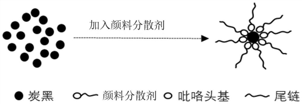
The invention is applicable to the technical field of display, and particularly provides a photoresist, a display substrate and a display panel, the photoresist contains at least one pigment dispersant shown in the following formula (I): (I), A comprises alkylene or alkenylene; z comprises carboxyl, hydroxyl, sulfydryl, substituted alkyl, and one or more of substituted or unsubstituted alkoxy, alkenyl, alkenyloxy, ester group and acyl, substituent groups in the substituted alkyl and alkenyl comprise at least one of carboxyl, hydroxyl and sulfydryl, and substituent groups in the substituted alkyl and alkenyl comprise at least one of carboxyl, hydroxyl and sulfydryl. Substituent groups in substituted alkoxy, alkenyloxy, acyl and ester groups comprise at least one of carboxyl, hydroxyl, sulfydryl and alkoxy. The pyrrole group of the pigment dispersant has high affinity to black pigments such as carbon black, and the Z group has good dispersibility in a photoresist solvent, so that the pigment dispersant can significantly improve the dispersibility of the black pigments in photoresist.

Description

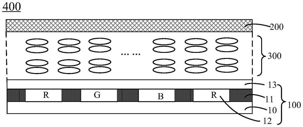
technical field [0001] The present application relates to the field of display technology, in particular to a photoresist, a display substrate and a display panel. Background technique [0002] A thin film transistor liquid crystal display (Thin Film Transistor-Liquid Crystal Display, TFT-LCD) mainly includes a TFT substrate and a CF (Color Filter, color filter) substrate arranged opposite to each other and a liquid crystal layer between the two, which is passed The electrical signal controls the switch of a thin film transistor (Thin Film Transistor, TFT) to control the deflection of the liquid crystal molecules to realize picture display. Among them, the CF substrate mainly provides the three primary colors for panel color display, and the color resists of the three primary colors usually need to be separated by a black matrix (BM) to avoid cross-color. [0003] BM is generally obtained by exposing and developing a negative photoresist containing photopolymerizable substa...

Claims


Application Information

Patent Timeline
Patent Type & Authority Applications(China)
IPC IPC(8): G03F7/004G03F7/027G02F1/1333
CPCG03F7/004G03F7/027G02F1/1333
Inventor 姜庆廖辉华杨文萍李荣荣
Owner CHANGSHA HKC OPTOELECTRONICS CO LTD
Learn More