
Circuit for configuring, reading back and refreshing SRAM (Static Random Access Memory) type FPGA (Field Programmable Gate Array) and operation method

A circuit and configuration data technology, applied in the direction of instruments, computer control, simulators, etc., can solve the problems of fixed single function, circuit function error, and configuration information lost when power is turned off, so as to overcome the fixed single function and enhance adaptability. Effect

Pending Publication Date: 2022-03-25
合肥腾芯微电子有限公司
View PDF2 Cites 4 Cited by
  • Summary
  • Abstract
  • Description
  • Claims
  • Application Information

AI Technical Summary

Problems solved by technology

However, SRAM-type FPGAs have a disadvantage: when FPGAs are used in harsh environments such as irradiation environments and artificial satellites, the SRAM storage cells in the Configuration SRAM array are susceptible to charged particles, false flips, 0, 1 data An error occurs, which in turn causes the user circuit function of the FPGA to malfunction
This method can realize the configuration and readback of the FPGA, but the disadvantage is that the configuration information will be lost when the power is turned off. It is only suitable for debugging and cannot be used for on-site deployment of products and equipment.
Another method is: use the PROM to load the configuration when the FPGA is powered on. The advantage is that the PROM can store the configuration data in a non-volatile manner, and since the upper computer is not required in the working state, it can be deployed in the actual product. However, its disadvantage is that it can only load the configuration of the power-on configuration to the FPGA, and cannot read back, compare, and refresh the FPGA configuration.
[0007] After retrieval, Chinese Patent Publication No. CN202011191407.9 discloses a dynamic refresh method and device for SRAM-type FPGA configuration data. This patent has the following defects: it only supports SPI NOR Flash, has a single fixed function, and cannot adjust and set the working mode of the chip in real time.
Chinese Patent Publication No. CN202011420884.8 discloses an IP core for on-board SRAM FPGA configuration and refresh control. This patent has the following defects: it only supports parallel port NOR Flash, the function is fixed and single, and the working mode of the chip cannot be adjusted in real time. set up
[0009] (1) The configuration of SRAM-type FPGA SRAM array is susceptible to the influence of space particles, cosmic rays, and charged particles, and then false flips occur
[0010] (2) The JTAG configuration method cannot carry out the actual deployment of the product on site
[0011] (2) The PROM mode cannot be read back and refreshed

Method used


Image

  • Circuit for configuring, reading back and refreshing SRAM (Static Random Access Memory) type FPGA (Field Programmable Gate Array) and operation method
  • Circuit for configuring, reading back and refreshing SRAM (Static Random Access Memory) type FPGA (Field Programmable Gate Array) and operation method
  • Circuit for configuring, reading back and refreshing SRAM (Static Random Access Memory) type FPGA (Field Programmable Gate Array) and operation method

Examples


Embodiment 1

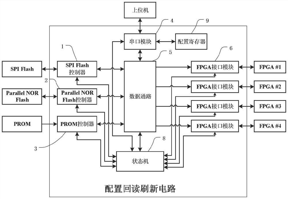
[0072] Depend on figure 1 As shown, a circuit for configuring, reading back and refreshing SRAM FPGA, the circuit includes the following components: SPI Flash controller 1, parallel port NOR Flash controller 2, PROM controller 3, serial port module 4, data path 5, FPGA interface module 6, state machine 8, configuration register 9.

[0073] The SPI Flash controller 1, the parallel port NOR Flash controller 2, and the PROM controller 3 are all memory controllers.

[0074] The SPI Flash controller 1 and the data path 5 carry out two-way data interaction; the SPI Flash controller 1 receives the data sent by the serial port module 4 through the data path 5 and writes it to the SPI Flash; the SPI Flash controller 1 reads The data in the SPI Flash is sent to the serial port module 4 or the FPGA interface module 6 through the data path 5; the SPIFlash controller 1 accepts the control of the state machine 8, and under the control of the state machine 8, the parallel port SPI Flash is ...

Embodiment 2

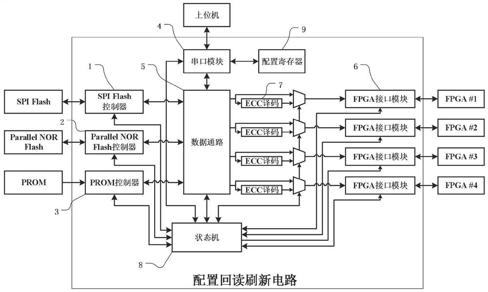
[0091] In order to improve the reliability of the system, on the basis of embodiment 1, by figure 2 As shown, the ECC decoding module 7 is inserted into the circuit: that is, a circuit for configuring, reading back and refreshing the SRAM FPGA, the circuit includes: SPI Flash controller 1, parallel port NOR Flash controller 2, PROM controller 3. Serial port module 4, data path 5, FPGA interface module 6, ECC decoding module 7, state machine 8.

[0092] Described ECC decoding module 7 is connected with FPGA interface module 6;

[0093] When writing data into SPI Flash / NOR Flash / PROM, firstly encode the data with ECC (ErrorCorrection Code), that is, add an error correction and detection code, and then write the encoded data into the corresponding memory. In the present invention, the error correction and error detection code can be added by the user outside the circuit using software in the computer, or can be added by the storage controller inside the circuit. If it is added ...

Embodiment 3

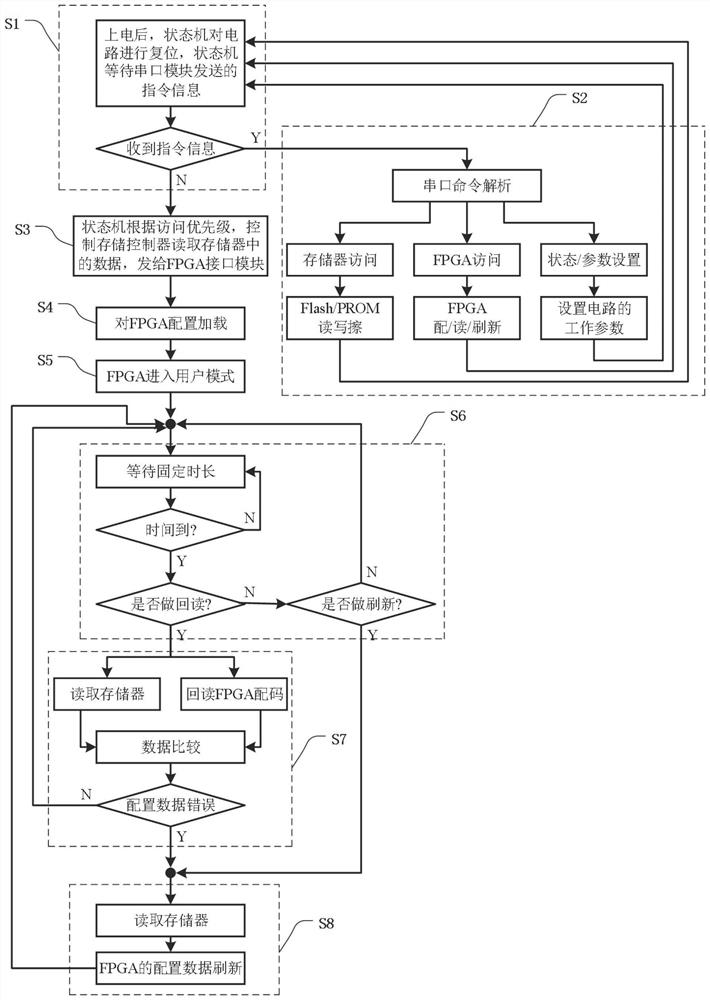
[0098] Based on the circuit structure provided by embodiment 1, by image 3 Shown, a kind of operation method that SRAM type FPGA is configured, read back and refresh of the present invention is as follows:

[0099] S1, after power on, the state machine 8 resets the circuit, then the state machine 8 waits for the instruction information sent by the serial port module 4, and judges whether the instruction information sent by the serial port module 4 is received, that is, the instruction information of the host computer. If the instruction is received, then Execute step S2; if no instruction is received, execute step S3;

[0100] S2, after the state machine 8 receives the command sent by the serial port module 4, that is, the command information of the upper computer, it parses the command, and performs corresponding operations according to the command parsing content:

[0101] If the instruction analysis content is to access the memory, that is, access SPI Flash / NOR Flash / PROM...


PUM


Abstract

The invention discloses a circuit for configuring, reading back and refreshing an SRAM (Static Random Access Memory) type FPGA (Field Programmable Gate Array). The circuit comprises a storage controller, a serial port module, a data path, an FPGA interface module, a state machine and a configuration register, the storage controller reads data in the memory and sends the data to the serial port module or the FPGA interface module through a data path; the serial port module is in two-way communication connection with the upper computer; the FPGA interface module receives data in the memory or data of the serial port module through a data path, and configures, reads back and refreshes the FPGA; the circuit disclosed by the invention can be used for detecting and updating code matching errors in an SRAM type FPGA (Field Programmable Gate Array) chip, and the adaptability of the FPGA to a severe environment is enhanced. And the circuit adopts the serial port module to receive information of an upper computer, so that the circuit can work according to a default predetermined flow after being powered on, and the working state of the circuit can be monitored through the serial port module to set and adjust the working mode.

Description

technical field [0001] The invention relates to the technical field of integrated circuits, in particular to a circuit and an operation method for configuring, reading back and refreshing an SRAM FPGA. Background technique [0002] FPGA is Field Programmable Gate Array, which is a general-purpose integrated circuit paralleled with CPU and DSP. The FPGA chip includes resources such as sequential logic, combinational logic, wiring resources, memory array, operational logic array, clock network, IO logic, etc. Users can design the FPGA through graphical design or hardware description language (HDL) design input. On-chip resources are called, and then various digital circuits are built. [0003] After the user completes the FPGA function development and design, the circuit design needs to be converted into a binary code stream. The code stream only contains 0 and 1 digital combinations. The different digital combinations determine the circuit structure in the FPGA chip. Since ...

Claims


Application Information

Patent Timeline
Patent Type & Authority Applications(China)
IPC IPC(8): G05B19/042
CPCG05B19/0423G05B2219/25257
Inventor 不公告发明人
Owner 合肥腾芯微电子有限公司
Learn More