Differential transmission structure based on BGA solder balls

A differential transmission and differential transmission line technology, applied in the direction of electrical components, electrical solid devices, circuits, etc., can solve the problems of increased insertion loss and return loss, thermal expansion mismatch, etc., to reduce insertion loss and return loss, reduce Effects of Thermal Expansion Mismatch, Low Dielectric Constant, and Dielectric Loss

Pending Publication Date: 2022-03-25
THE 13TH RES INST OF CHINA ELECTRONICS TECH GRP CORP
View PDF0 Cites 0 Cited by
  • Summary
  • Abstract
  • Description
  • Claims
  • Application Information

AI Technical Summary

Problems solved by technology

[0006] The purpose of the present invention is to provide a differential transmission structure based on BGA solder balls, which aims to solve the traditional packaging process, which usually adopts the structural form of PCB board-BGA solder balls-LTCC substrate. In the process of actually transmitting signals, transmission With the increase of the application frequency of the signal, the insertion loss and return loss increase rapidly, and it is also accompanied by the problem of thermal expansion mismatch

Method used


Image

  • Differential transmission structure based on BGA solder balls
  • Differential transmission structure based on BGA solder balls
  • Differential transmission structure based on BGA solder balls

Examples


Embodiment Construction

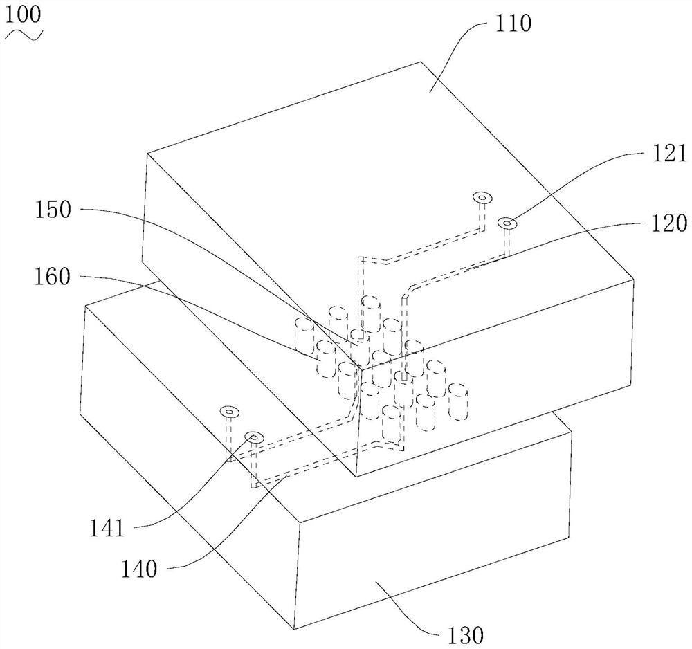
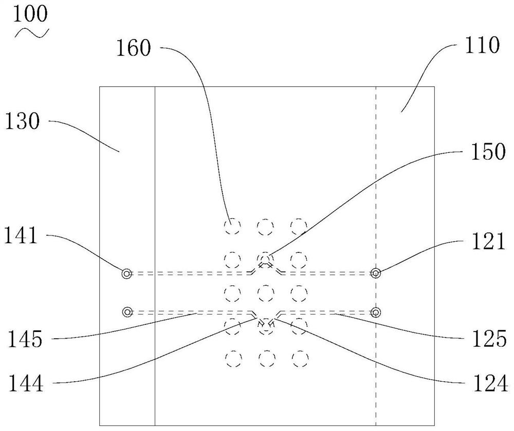
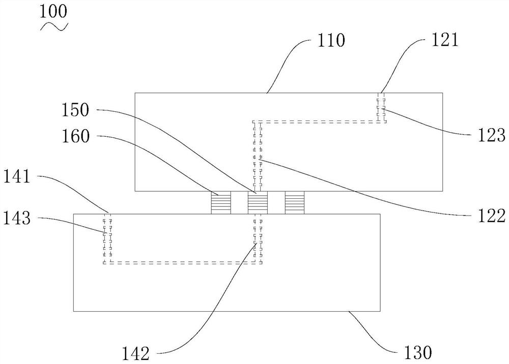
[0033] In order to make the technical problems, technical solutions and beneficial effects to be solved by the present invention clearer, the present invention will be further described in detail below in conjunction with the accompanying drawings and embodiments. It should be understood that the specific embodiments described here are only used to explain the present invention, not to limit the present invention.

[0034] It should be noted that when an element is considered to be "connected to" or "connected" to another element, it may be directly connected to the other element or there may be an intervening element at the same time. When an element is referred to as being "disposed on", "provided on" or "fixed on" another element, it can be directly on the other element or intervening elements may also be present. "Plurality" refers to two or more quantities.

[0035] Unless otherwise defined, all technical and scientific terms used herein have the same meaning as commonly...


PUM

PropertyMeasurementUnit
thicknessaaaaaaaaaa
diameteraaaaaaaaaa

Abstract

The invention provides a differential transmission structure based on BGA solder balls, and belongs to the technical field of ceramic packaging. The two upper differential transmission lines are arranged at intervals and penetrate from the upper surface of the HITCE upper substrate to the lower surface of the HITCE upper substrate, and upper test points are formed on the upper surface of the HITCE upper substrate; the HITCE lower substrate and the HITCE upper substrate are arranged in a stacked manner; the two lower differential transmission lines are arranged at intervals, are bent and extend in the thickness direction of the HITCE lower substrate from the upper surface of the HITCE lower substrate, and penetrate out of the upper surface of the HITCE lower substrate to form lower test points; the signal transmission solder ball is arranged between the HITCE upper substrate and the HITCE lower substrate, and the upper differential transmission line and the lower differential transmission line are connected through the signal transmission solder ball; and the plurality of grounding solder balls are arranged around the signal transmission solder balls and are connected with the backflow ground layers in the HITCE upper substrate and the HITCE lower substrate.

Description

technical field [0001] The invention belongs to the technical field of ceramic packaging, and more specifically relates to a differential transmission structure based on BGA solder balls. Background technique [0002] The rapid development of microwave and millimeter wave radar, communication, electronic warfare and other systems has brought about the generation of massive data, which has brought a lot of demand for integrated circuit chips with functions such as high-speed data transmission, high-speed data processing and data storage. Microwave and millimeter wave packaging Technology is facing issues such as signal integrity and high heat dissipation brought about by high frequency, high speed, and high power. [0003] The BGA highly integrated SIP based on multilayer co-fired ceramics is considered to be a promising packaging form, which can meet the needs of components for high-frequency and high-speed microsystem packaging. At present, most high-frequency chips work i...

Claims


Application Information

Patent Timeline
Patent Type & Authority Applications(China)
IPC IPC(8): H01L23/15H01L23/58H01L23/49H01L23/488
CPCH01L23/15H01L23/58H01L23/49H01L24/13H01L2224/13
Inventor 余希猛杨振涛段强高岭杨德明鮑禹希
Owner THE 13TH RES INST OF CHINA ELECTRONICS TECH GRP CORP
Why Eureka
Try Eureka