Mg-doped enhanced transition metal sulfide-based visible light detector and preparation method thereof
A technology of transition metals and sulfides, applied in sustainable manufacturing/processing, semiconductor devices, climate sustainability, etc., can solve problems such as the difficulty of forming a strong heterojunction built-in electric field, so as to improve device performance and reduce dark Current, the effect of improving the response speed
- Summary
- Abstract
- Description
- Claims
- Application Information
AI Technical Summary
Problems solved by technology
Method used
Image
Examples
Embodiment 1
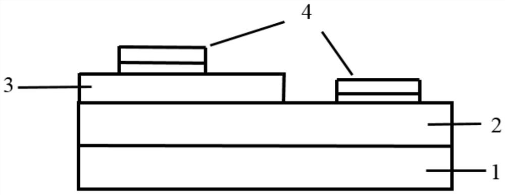
[0047] This embodiment provides a Mg-doped enhanced transition metal dichalcogenide (TMDs) based visible light detector, comprising a Si substrate layer, an InGaN layer, a Mg-doped TMDs layer, a Ti electrode layer and a gold electrode layer from bottom to top .
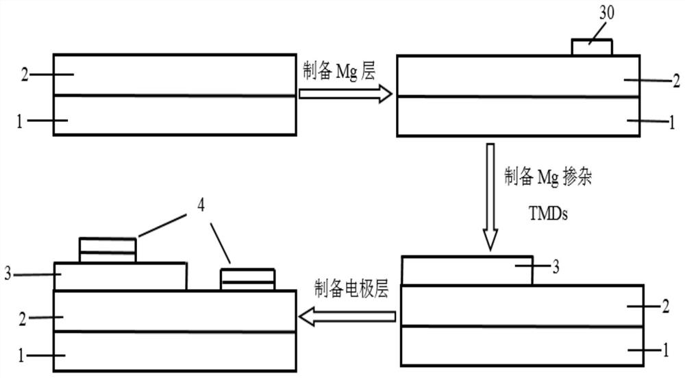
[0048] This embodiment also provides a method for preparing a Mg-doped enhanced transition metal dichalcogenide (TMDs)-based visible light detector, comprising the following steps:
[0049] 1) Spin-coat photoresist on the Si-based InGaN epitaxial wafer, and photoetch the Mg layer evaporation area device (the Mg evaporation area is located at one end of the upper surface of the InGaN epitaxial wafer, partially covering InGaN);
[0050] 2) Evaporating a layer of metal Mg with molecular beam evaporation equipment on the evaporation area of step 1), the thickness of the metal Mg is 10nm, to obtain an epitaxial wafer device containing a metal Mg layer;
[0051] 3) stripping and cleaning the unexposed photoresist of the ...
Embodiment 2
[0060] This embodiment provides a Mg-doped enhanced transition metal dichalcogenide (TMDs) based visible light detector, comprising a Si substrate layer, an InGaN layer, a Mg-doped TMDs layer, a Ti electrode layer and a gold electrode layer from bottom to top .
[0061] This embodiment also provides a method for preparing a Mg-doped enhanced transition metal dichalcogenide (TMDs)-based visible light detector, comprising the following steps:
[0062] 1) Spin-coat photoresist on the Si-based InGaN epitaxial wafer, and photoetch the evaporation area of the Mg layer; the evaporation area is located at one end of the upper surface of the InGaN layer;
[0063] 2) Evaporating a layer of metal Mg with molecular beam evaporation equipment on the evaporation area of step 1), the thickness of the metal Mg is 20nm, to obtain an epitaxial wafer device containing a metal Mg layer;
[0064] 3) stripping and cleaning the unexposed photoresist of the device containing the metal Mg layer d...
Embodiment 3
[0071] This embodiment provides a Mg-doped enhanced transition metal dichalcogenide (TMDs)-based visible light detector, including a Si substrate layer, an InGaN layer, and a Mg-doped MoS layer from bottom to top. 2 layer, Ti electrode layer and Au electrode layer.
[0072] This embodiment also provides a method for preparing a Mg-doped enhanced transition metal dichalcogenide (TMDs)-based visible light detector, comprising the following steps:
[0073] 1) Spin-coat photoresist on the Si-based InGaN epitaxial wafer, and photoetch the Mg layer evaporation area device;
[0074] 2) Evaporating a layer of metal Mg with molecular beam evaporation equipment for the device in step 1), the thickness of the metal Mg is 50nm, to obtain an epitaxial wafer device containing a metal Mg layer;
[0075] 3) stripping and cleaning the unexposed photoresist of the device containing the metal Mg layer described in step 2) to obtain the stripped Mg layer device;
[0076] 4) For the Mg layer dev...
PUM
| Property | Measurement | Unit |
|---|---|---|
| Doping concentration | aaaaa | aaaaa |
| Thickness | aaaaa | aaaaa |
| Thickness | aaaaa | aaaaa |
Abstract
Description
Claims
Application Information


