
Electromagnetic wave broadband selective absorption micro-nano structure and preparation method thereof

A micro-nano structure and selective technology, applied in the field of infrared stealth, can solve the problem of limited electromagnetic wave broadband selective radiation micro-nano structure application, high-efficiency manufacturing, positive cone electromagnetic resonance structure and patterned multi-scale coplanar unit period structure cannot be large Area and other issues, to achieve the effect of large-area manufacturing and high consistency

Pending Publication Date: 2022-04-01
NANJING UNIV OF AERONAUTICS & ASTRONAUTICS
View PDF5 Cites 3 Cited by
  • Summary
  • Abstract
  • Description
  • Claims
  • Application Information

AI Technical Summary

Problems solved by technology

[0003] However, due to design defects and limitations in processing forms, the performance of electromagnetic broadband selective radiation micro-nano structures and their processing technology are limited, resulting in the design of positive cone electromagnetic resonance structures and patterned multi-scale coplanar unit periodic structures. manufacturing, which greatly limits the application of electromagnetic wave broadband selective radiation micro-nano structures in infrared stealth and radiation heat dissipation

Method used


Image

  • Electromagnetic wave broadband selective absorption micro-nano structure and preparation method thereof
  • Electromagnetic wave broadband selective absorption micro-nano structure and preparation method thereof
  • Electromagnetic wave broadband selective absorption micro-nano structure and preparation method thereof

Examples


Embodiment 1

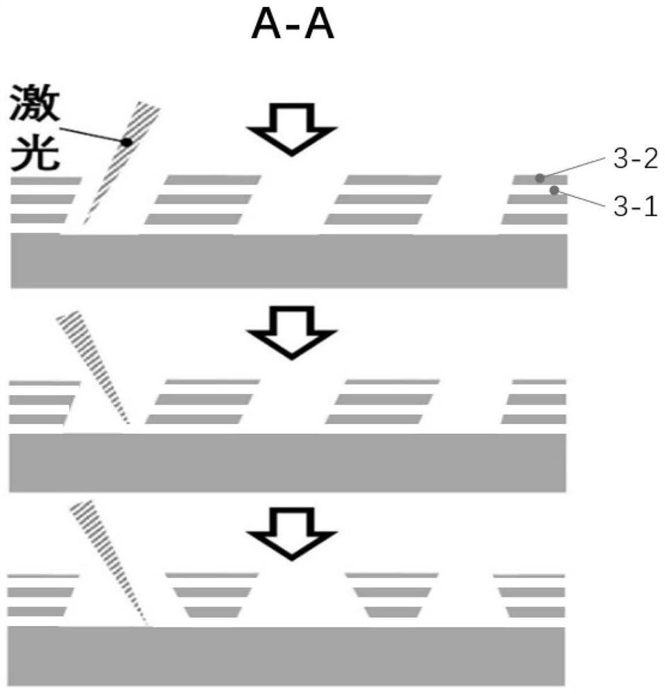
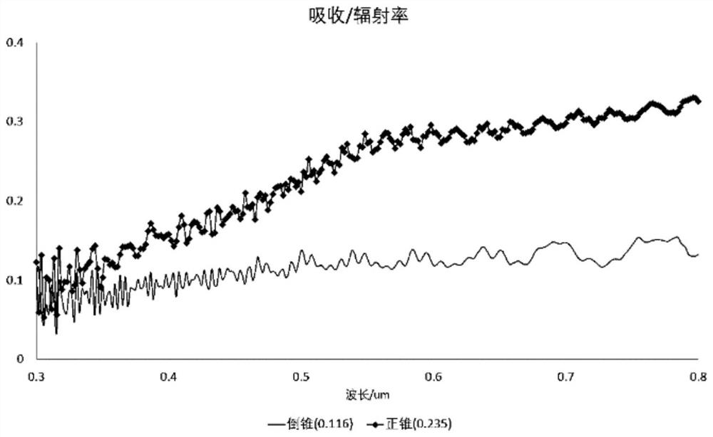
[0041] Such as figure 1 As shown, this embodiment provides an electromagnetic wave broadband selective absorption micro-nano structure with an inverted cone periodic structure. Absorbent properties.

[0042] The micro-nano structure uses silicon as the matrix 1 . On the substrate 1 is a reflector 2, and the reflector 2 is a silver layer. The absorber 3 is on the reflector 2, and the absorber 3 is a forward cone (contrast) / inverted cone periodic structure, and the forward cone / inverted cone periodic structure is a structure formed by a number of forward cones / inverted cones arranged periodically in a matrix , the forward cone / inverted cone monomer is formed by overlapping at least two groups of metal layers and dielectric layers. Layer 3-1, silver layer as metal layer 3-2.

[0043] In the micro-nano structure in which the absorber 3 is a positive cone periodic structure, the thickness of the reflector 2 is 0.15 μm, the thickness of the germanium layer of the absorber 3 is 0...

Embodiment 2

[0057] Such as Figure 5As shown in (b), this embodiment provides an electromagnetic wave broadband selective absorption micro-nano structure with an arrayed multi-scale coplanar unit periodic structure with a discontinuous dielectric layer. Copper is used as the substrate 4, and the reflector 5 is formed on the substrate 4, and the reflector 5 is a silver layer. The absorber 6 is on the reflector 5, and the absorber 6 is an arranged multi-scale coplanar unit periodic structure of a discontinuous dielectric layer, which is a structure formed by a periodic arrangement of several dielectric-metal square units, wherein the dielectric-metal square The unit is composed of a number of dielectric-metal squares of different sizes arranged periodically in a matrix. The dielectric-metal square is a layered square structure containing two layers. The lower layer is a dielectric layer 6-1 and the upper layer is a metal layer 6-2. Among them, Such as Figure 6 As shown, the column direct...

Embodiment 3

[0066] Such as Figure 5 As shown in (a), this embodiment provides an electromagnetic wave broadband selective absorption micro-nano structure with an arrayed multi-scale coplanar unit periodic structure with a continuous dielectric layer. Specifically, it has a "gold-zinc sulfide-superalloy K424 "structure. The gold, zinc sulfide and K424 superalloy used in the structure of this embodiment can all withstand above 1000°C, so this electromagnetic wave broadband selective absorption radiation micro-nano structure can work in a high-temperature environment, and can be used as a high-performance infrared stealth in a high-temperature environment , Design case of radiative cooling compatible micro-nano structure. The micro-nano structure uses superalloy K424 as the matrix. The substrate is a reflector, and the reflector is a gold layer. The absorber is on the reflector, and the absorber is an arrangement type multi-scale coplanar unit periodic structure of a continuous dielectri...


PUM

PropertyMeasurementUnit
thicknessaaaaaaaaaa
thicknessaaaaaaaaaa
thicknessaaaaaaaaaa

Abstract

The invention discloses an electromagnetic wave broadband selective absorption micro-nano structure and a preparation method thereof. The micro-nano structure comprises a substrate, a reflector and an absorber which are continuously connected, the base material is a dielectric medium or metal; the reflector is a metal layer and covers the substrate; the absorber is located above the reflector and is of an inverted cone periodic structure or an arrangement type multi-scale coplanar unit periodic structure formed by overlapping a metal layer and a dielectric layer; wherein the inverted cone periodic structure is a structure formed by periodically arranging a plurality of inverted cone monomers in a matrix, each inverted cone monomer is formed by overlapping at least two groups of metal layers and dielectric layers, and the top layer is a metal layer; the arrangement type multi-scale coplanar unit periodic structure is an arrangement type multi-scale coplanar unit periodic structure of a continuous dielectric layer or an arrangement type multi-scale coplanar unit periodic structure of a discontinuous dielectric layer. The plasma broadband selective absorption micro-nano structure disclosed by the invention can be used for compatible design of infrared stealth and radiation cooling.

Description

technical field [0001] The invention belongs to the field of infrared stealth and relates to a structure with infrared stealth performance, in particular to an electromagnetic wave broadband selective absorption micro-nano structure and a preparation method thereof. Background technique [0002] With the development of infrared detection technology, the problem of infrared stealth of military targets has become increasingly prominent. Therefore, research on infrared stealth technology, changing the detectability of targets through various technical means, and reducing the ability of the detection system to identify and lock targets is crucial to improving military competitiveness. important. According to the Stefan-Boltzmann law, the total radiant energy of an object is proportional to the first power of the average emissivity of the object and the fourth power of the absolute temperature. Therefore, reducing the average emissivity and temperature of the object is the key to...

Claims


Application Information

Patent Timeline
Patent Type & Authority Applications(China)
IPC IPC(8): G02B5/00G02B5/28
Inventor 杨晓龙郭何涛朱荻桓恒于真鹤程玉贤
Owner NANJING UNIV OF AERONAUTICS & ASTRONAUTICS
Learn More