Electron extraction type freewheel diode device and preparation method thereof

A freewheeling diode and device technology, which is applied to the structure of an electron extraction type freewheeling diode device and the field of its preparation, can solve problems such as the limitation of the adjustment range of hole injection efficiency, and achieves reduction of manufacturing cost, reduction of process difficulty, and increase of adjustment. Amplitude effect

Active Publication Date: 2022-04-08
安建科技(深圳)有限公司
View PDF9 Cites 5 Cited by
  • Summary
  • Abstract
  • Description
  • Claims
  • Application Information

AI Technical Summary

Problems solved by technology

However, the adjustment of the Schottky barrier height is limited by the P-type withstand voltage and on-resistance, and the adjustment range of the hole injection efficiency is limited.

Method used


Image

  • Electron extraction type freewheel diode device and preparation method thereof
  • Electron extraction type freewheel diode device and preparation method thereof
  • Electron extraction type freewheel diode device and preparation method thereof

Examples


Embodiment 1

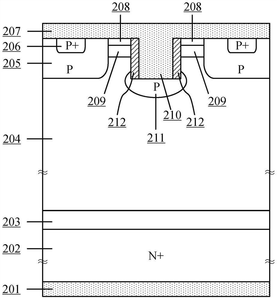
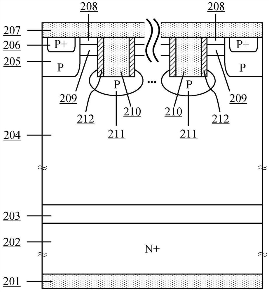
[0044] figure 2 It is a cross-sectional schematic view of the device structure of the vertical trench electron extraction type freewheeling diode according to the first embodiment of the present invention. The device structure has: a cathode electrode 201 at the bottom, a heavily doped N-type semiconductor substrate 202 and an N-type buffer layer 203 above the cathode electrode 201, and an N-type drift region 204 is located on the N-type buffer layer 203; The upper surface of the N-type drift region 204 has a P-type planar anode region 205, a lightly doped P-type base region 209, and a P-type trench anode region 211. The upper surface of the P-type planar anode region 205 has a partially heavily doped P-type ohmic region. Contact region 206; the upper surface of the lightly doped P-type base region 209 has a heavily doped N-type emitter region 208; the P-type planar anode region 205 and the heavily doped N-type emitter region The region 209 is adjacent, and the P-type planar...

Embodiment 2

[0058] Figure 4 is an enlarged cross-sectional view of a device according to a second embodiment of the present invention. compared to figure 2 The difference between the device structure in the first embodiment and the device structure in the second embodiment is that a slope trench structure is used. The shape of the slope trench region 310 is an inverted trapezoid, the angle between the side wall and the vertical direction can be 60-90°, and the side wall is completely surrounded by the heavily doped N-type emitter region, forming an ohmic contact with the anode electrode. When the position of the punch-through NPN transistor is adjusted from adjacent to the groove gate to the side wall of the slope groove gate, the conductive area of ​​the anode will be effectively increased, which is beneficial to reduce the conduction voltage drop and improve the forward anti-surge current capability of the device. With the increase of the slot gate density, the electron extraction a...

Embodiment 3

[0070] Figure 6 is an enlarged cross-sectional view of the device according to the third embodiment of the present invention. compared to figure 2 The difference between the device structure shown in the first embodiment and the device structure in the third embodiment is that the area of ​​the anode P-type region is increased. The anode electrode 407 is simultaneously connected to the side wall of the vertical groove area 410 and the P-type groove anode area 411. The P-type groove anode area 411 surrounds the left and right side walls and the bottom of the vertical groove area 410. The anode electrode 407 and The P-type trench anode region 411 forms a Schottky contact. This structure increases the conductive area of ​​the P-type region, helps to control the anode hole injection efficiency, and also narrows the JFET conductive channel, enhances its shielding effect on high electric fields, and helps reduce leakage current at high temperatures .

[0071] in the same cell,...


PUM


Abstract

The invention discloses an electron extraction type freewheel diode device and a preparation method thereof, and relates to a power semiconductor device. More than one first structure for increasing the density of an electron extraction path is also arranged on an N-type drift region; the first structure comprises a lightly doped P-type base region, a heavily doped N-type emitter region, a P-type trench anode region and a trench region, the heavily doped N-type emitter region and the P-type trench anode region are arranged above the lightly doped P-type base region, the trench region is arranged on the P-type trench anode region, and the heavily doped N-type emitter region, the lightly doped P-type base region and the N-type drift region form a punch-through NPN triode structure; the N-type drift region, the P-type planar anode region and the P-type trench anode region form a JFET structure, the P-type planar anode region and the P-type trench anode region form Schottky contact with the anode electrode, and the heavily doped P-type ohmic contact region forms ohmic contact with the anode electrode; and the adjustment range of the potential barrier height of the punch-through NPN triode is wide, and the adjustment range of soft and fast reverse recovery can be increased.

Description

technical field [0001] The invention relates to a power semiconductor device, in particular to the structure of an electron extraction type freewheeling diode device and its preparation method. Background technique [0002] In order to reduce carbon emissions and achieve "carbon neutrality", the fields of photovoltaic power generation, electric vehicles and intelligent rail transit have developed rapidly in recent years, and power semiconductor devices represented by IGBT (Insulated gate bipolar transistor, insulated gate bipolar transistor) have been developed. large-scale application. With the characteristics of easy gate drive, high power density and fast switching speed, IGBT can effectively improve the energy utilization rate of motor drive and power conversion. The hard switching mode has the advantages of simple drive circuit structure and easy cost control, and has become a common switching mode for IGBTs in inductive load applications. In inductive load applicatio...

Claims


Application Information

Patent Timeline
IPC IPC(8): H01L29/861H01L27/07H01L29/06H01L21/329
CPCH01L29/1608H01L29/861H01L29/66136H01L29/0603H01L29/8725H01L29/063H01L29/0657H01L29/66143H01L21/266H01L21/30655H01L21/26513
Inventor 冯浩刘永单建安
Owner 安建科技(深圳)有限公司
Why Eureka
Try Eureka