Light emitting diode and preparation method thereof

A technology of light-emitting diodes and light-emitting layers, which is applied to electrical components, circuits, semiconductor devices, etc., can solve the problems of low electron-hole radiation recombination efficiency and hole injection efficiency, and achieve enhanced radiation recombination efficiency and increased hole concentration , increase the effect of hole injection

Pending Publication Date: 2022-04-12
HUAIAN AUCKSUN OPTOELECTRONICS TECHNOLOGY CO LTD
View PDF10 Cites 2 Cited by
  • Summary
  • Abstract
  • Description
  • Claims
  • Application Information

AI Technical Summary

Problems solved by technology

It solves the technical problem of low electron-hole radiation recombination efficiency in quantum wells due to low hole injection efficiency in the prior art

Method used


Image

  • Light emitting diode and preparation method thereof
  • Light emitting diode and preparation method thereof
  • Light emitting diode and preparation method thereof

Examples


preparation example Construction

[0080] The present invention also provides a method for preparing the light-emitting diode as described above, comprising the following steps:

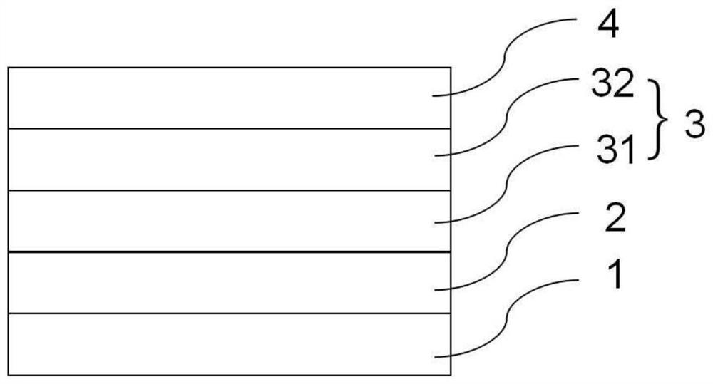
[0081] growing an N-type semiconductor layer 2, a multi-quantum well light-emitting layer 3 and a P-type semiconductor layer 4 sequentially on the surface of the substrate 1 to obtain the light-emitting diode;

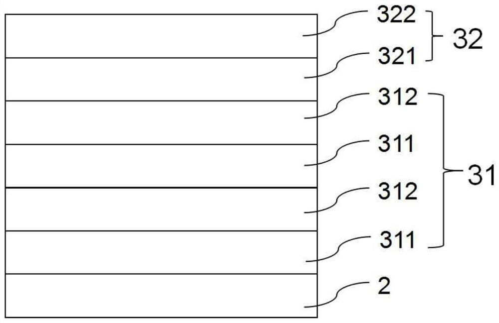
[0082] Wherein, the preparation method of the multi-quantum well light-emitting layer 3 specifically includes: periodically and alternately growing the first quantum well layer 311 and the quantum barrier layer 312 on the surface of the N-type semiconductor layer 2 to obtain the first sub-layer 31; and then growing a second quantum well layer 321 and a superlattice structure barrier layer 322 sequentially on the surface of the first sublayer 31 to obtain a second sublayer 32;

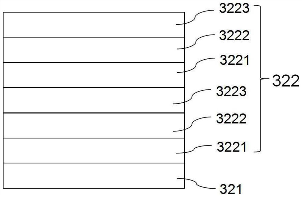
[0083] The superlattice structure barrier layer 322 includes a GaN layer 3221, an AlGaN layer 3222 and a P-type layer 3223 that are periodically and al...

Embodiment 1

[0133] The light emitting diode provided in this embodiment includes: a substrate 1 (sapphire substrate 1 ), and an N-type semiconductor layer 2 , a multi-quantum well light-emitting layer 3 and a P-type semiconductor layer 4 sequentially stacked on the surface of the substrate 1 . Its structure can be found in Figure 4 .

[0134] Among them, such as Figure 5 As shown, the multi-quantum well light-emitting layer 3 includes a first sublayer 31 and a second sublayer 32 sequentially stacked on the surface of the N-type semiconductor layer 2; the first sublayer 31 is included in the N-type semiconductor layer 2 The surface of the type semiconductor layer 2 is a first quantum well layer 311 (InGaN) and a quantum barrier layer 312 (GaN) that are alternately stacked in 5 cycles; the second sublayer 32 is composed of The second quantum well layer 321 (InGaN) and the superlattice structure barrier layer 322 are stacked.

[0135] like Figure 6 As shown, the superlattice barrier l...

Embodiment 2

[0152] The structure of the light emitting diode provided by this embodiment is basically the same as that of Embodiment 1, the difference is:

[0153] First, the superlattice structure barrier layer 322 includes GaN layers 3221, AlGaN layers 3222, and P-type layers 3223 that are alternately stacked in three cycles; wherein, the P-type layers in the first cycle and the second cycle Layer 3223 is an AlGaN layer doped with P-type dopants (AlGaN layer doped with Mg), and the P-type layer 3223 in the third period (ie, the last period, the last barrier layer) is doped with P-type dopant agent GaN layer (GaN layer doped with Mg).

[0154] Second, the alternating cycle of the first sub-layer 31 is 8.

[0155] Third, the GaN layer 3221 in the superlattice structure barrier layer 322 has a thickness of 2.1 nm, the AlGaN layer 3222 has a thickness of 0.5 nm, and the P-type layer 3223 has a thickness of 0.5 nm.

[0156] The preparation method of the light-emitting diode provided in thi...


PUM

PropertyMeasurementUnit
thicknessaaaaaaaaaa
thicknessaaaaaaaaaa
thicknessaaaaaaaaaa

Abstract

The invention relates to the technical field of semiconductors, in particular to a light-emitting diode and a preparation method thereof. The light-emitting diode comprises a substrate, an N-type semiconductor layer, a multi-quantum well light-emitting layer and a P-type semiconductor layer, wherein the multi-quantum well light-emitting layer comprises a first sub-layer and a second sub-layer; the first sub-layer comprises a first quantum well layer and a quantum barrier layer; the second sub-layer comprises a second quantum well layer and a superlattice structure barrier layer; the superlattice structure barrier layer comprises a GaN layer, an AlGaN layer and a P-type layer which are periodically, sequentially and alternately stacked; the P-type layer comprises an AlGaN layer doped with a P-type dopant and/or a GaN layer doped with a P-type dopant. The GaN/AlGaN/P-type layer superlattice structure is arranged in the second sub-layer, so that two-dimensional electron gas can be formed, current expansion is improved, electron overflow is blocked, hole injection is increased, and the luminance of the LED is further improved.

Description

technical field [0001] The invention relates to the technical field of semiconductors, in particular to a light emitting diode and a preparation method thereof. Background technique [0002] A light-emitting diode (light-emitting diode, referred to as LED), is a light-emitting device that releases energy by recombining electrons and holes to emit light, and can efficiently convert electrical energy into light energy. With the development of science and technology, light-emitting diodes are now widely used in technical fields such as displays, lighting, and medical devices. [0003] However, in the light-emitting diodes in the prior art, there are lattice differences between the quantum well and the quantum barrier in the light-emitting layer, which often cause energy band bending, and electrons tend to overflow to the P-type region; on the other hand, the quantum well is hollow. The hole concentration is low, and the hole mobility is low, which will lead to the technical pr...

Claims


Application Information

Patent Timeline
Patent Type & Authority Applications(China)
IPC IPC(8): H01L33/06H01L33/14H01L33/32H01L33/00
Inventor 刘丽军刘康朱涛展望芦玲
Owner HUAIAN AUCKSUN OPTOELECTRONICS TECHNOLOGY CO LTD
Why Eureka
Try Eureka