Method for preparing tungsten on semiconductor wafer

A semiconductor and wafer technology, used in semiconductor/solid-state device manufacturing, coating, gaseous chemical plating, etc., can solve the problems of increased damage to the back of the wafer, deterioration, affecting product yield, etc., and reduce warpage. risk, protecting the backside of the wafer, reducing the effect of damage

Pending Publication Date: 2022-04-29
WUHAN XINXIN SEMICON MFG CO LTD
View PDF0 Cites 0 Cited by
  • Summary
  • Abstract
  • Description
  • Claims
  • Application Information

AI Technical Summary

Problems solved by technology

[0003] However, when chemical vapor deposition is used to deposit tungsten on one side of the semiconductor wafer (called the front or first surface), although the other side of the semiconductor wafer (called the back or the second surface) is placed on the base, the The morphology will also change, which is specifically reflected in the corrosion of the back of the wafer and the deterioration of the planarity. In the subsequent processes such as front planarization and crystal back cleaning, the degree of damage to the back of the wafer will be further aggravated, resulting in the final appearance of the back of the wafer. The color difference and flatness problem visible to the naked eye will affect the packaging process of subsequent semiconductor components and affect the product yield.

Method used


Image

  • Method for preparing tungsten on semiconductor wafer
  • Method for preparing tungsten on semiconductor wafer

Examples


Embodiment Construction

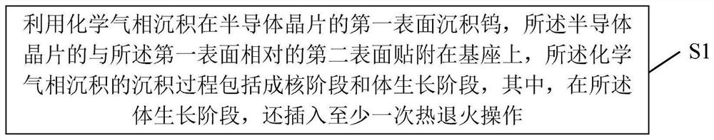
[0022] The method for preparing tungsten on a semiconductor wafer of the present invention will be further described in detail below in conjunction with the accompanying drawings and specific embodiments. The advantages and features of the present invention will become clearer from the following description. It should be understood that the drawings in the description are all in very simplified form and use imprecise scales, and are only used to facilitate and clearly assist the purpose of illustrating the embodiments of the present invention. It should be noted that the order of the steps in the methods presented herein is not necessarily the only order in which the steps are performed, some described steps may be omitted and / or some other steps not described herein may be added to the method.

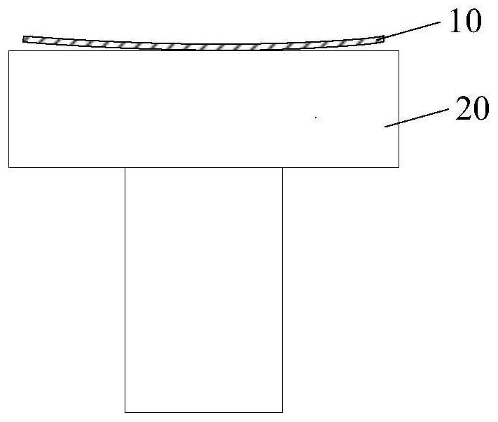
[0023] figure 1 is a schematic illustration of warping of a semiconductor wafer during tungsten chemical vapor deposition. refer to figure 1 , the semiconductor wafer 10 is placed ...


PUM


Abstract

The invention relates to a method for producing tungsten on a semiconductor wafer. According to the method, tungsten is deposited on a first surface of a semiconductor wafer through chemical vapor deposition, a second surface, opposite to the first surface, of the semiconductor wafer, namely the back face is attached to a base, and at least one time of thermal annealing operation is inserted in the body growth stage. By means of the thermal annealing operation, the stress accumulated by tungsten deposited on the semiconductor wafer can be relieved, the warping risk of the semiconductor wafer is reduced, damage of process gas of chemical vapor deposition to the back face of the semiconductor wafer is reduced, and the purpose of protecting the back face of the wafer is achieved.

Description

technical field [0001] The invention relates to the technical field of semiconductors, in particular to a method for preparing tungsten on a semiconductor wafer. Background technique [0002] Compared with tungsten deposited by physical sputtering, tungsten chemical vapor deposition has low resistivity, high resistance to electromigration, excellent planarity and excellent step coverage when filling small vias, At present, it has become an important technology in the semiconductor process. In the structure of semiconductor components, tungsten is usually used as a highly conductive interconnection metal, through silicon vias (Through Silicon Via, TSV) between metal layers and contact holes (Contact) for vertical contacts, and between aluminum and silicon. spacer layer. Common main process gases for tungsten chemical vapor deposition include tungsten hexafluoride (WF 6 ). [0003] However, when chemical vapor deposition is used to deposit tungsten on one side of the semic...

Claims


Application Information

Patent Timeline
Patent Type & Authority Applications(China)
IPC IPC(8): H01L21/02H01L21/768C23C16/06C23C16/56
CPCH01L21/02697H01L21/76838H01L21/76864C23C16/06C23C16/56
Inventor 李振亚王鹏王敏高尚
Owner WUHAN XINXIN SEMICON MFG CO LTD
Why Eureka
Try Eureka