Improved wet etching method for selectively removing silicon nitride

A technology of wet etching and silicon nitride, which is applied in the manufacture of electrical components, circuits, semiconductors/solid-state devices, etc., can solve the problems of reducing etching performance and wafer cross-contamination, achieve high selectivity, improve quality, and avoid impurities cumulative effect

Pending Publication Date: 2022-04-29
PNC PROCESS SYSTEMS CO LTD +1
View PDF0 Cites 0 Cited by
  • Summary
  • Abstract
  • Description
  • Claims
  • Application Information

AI Technical Summary

Problems solved by technology

Among them, reactive ion etching can be used for dry etching, however, reactive ion etching for silicon nitride lacks high selectivity to silicon oxide layer and will degrade silicon oxide layer or silicon substrate in the form of surface pitting; wet etching usually Etching is carried out in an acid bath, that is, the si

Method used


Image

  • Improved wet etching method for selectively removing silicon nitride
  • Improved wet etching method for selectively removing silicon nitride
  • Improved wet etching method for selectively removing silicon nitride

Examples


Example Embodiment

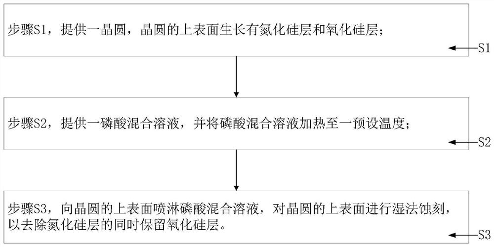
[0032] The present invention will be described in detail below with reference to the accompanying drawings and specific embodiments. The present invention is not limited to this embodiment, and other embodiments may belong to the scope of the present invention as long as it conforms to the gist of the present invention.

[0033] In a preferred embodiment of the present invention, based on the above problems existing in the prior art, an improved wet etching method for selectively removing silicon nitride is provided, such as figure 1 shown, including:

[0034] In step S1, a wafer is provided, and a silicon nitride layer and a silicon oxide layer are grown on the upper surface of the wafer;

[0035] Step S2, providing a phosphoric acid mixed solution, and heating the phosphoric acid mixed solution to a preset temperature;

[0036] In step S3, the phosphoric acid mixed solution is sprayed on the upper surface of the wafer, and the upper surface of the wafer is wet-etched to re...


PUM


Abstract

The invention provides an improved wet etching method for selectively removing silicon nitride, and relates to the technical field of semiconductors, and the method comprises the steps: S1, providing a wafer, and enabling a silicon nitride layer and a silicon oxide layer to grow on the upper surface of the wafer; s2, providing a phosphoric acid mixed solution, and heating the phosphoric acid mixed solution to a preset temperature; and S3, spraying the phosphoric acid mixed solution to the upper surface of the wafer, and performing wet etching on the upper surface of the wafer so as to remove the silicon nitride layer and reserve the silicon oxide layer at the same time. The method has the beneficial effects that phosphoric acid and ultrapure water are mixed to form a phosphoric acid mixed solution, the phosphoric acid mixed solution is heated to form a high-temperature phosphoric acid mixed solution, and selective cleaning and etching are performed by adopting a spraying mode, so that high selectivity is realized, impurity accumulation of the phosphoric acid mixed solution and cross infection of wafers are effectively avoided, and the quality of a prepared product is effectively improved.

Description

technical field [0001] The invention relates to the technical field of semiconductors, in particular to an improved wet etching method for selectively removing silicon nitride. Background technique [0002] The surface sacrificial layer technology refers to that in the process of forming the cavity of the micromechanical structure or the movable microstructure, first deposit various special structural parts required by structural materials on the underlying film, and then use chemical etchant to deposit the required special structures. The first layer of thin film is etched away, but the microstructure is not damaged, and then the upper thin film structure (cavity or microstructure) is obtained. Since the removed lower film only acts as a separation layer, it is called a sacrificial layer (thickness about 1-2 μm). In semiconductor devices, silicon nitride is often used as a sacrificial layer and is formed adjacent to or close to the silicon oxide layer. [0003] Existing m...

Claims


Application Information

Patent Timeline
IPC IPC(8): H01L21/311H01L21/02
CPCH01L21/31111H01L21/0206
Inventor 廖世保邓信甫黄茂烘陈丁堃
Owner PNC PROCESS SYSTEMS CO LTD
Why Eureka
Try Eureka