Supercharge Your Innovation With Domain-Expert AI Agents!

Deep ultraviolet semiconductor light-emitting element

A light-emitting element and semiconductor technology, applied in semiconductor devices, electrical components, circuits, etc., can solve the problems of AlGaN materials such as low Al mobility, low lateral growth rate, and easy cracks, so as to reduce lateral expansion ability and improve ESD resistance Ability to reduce the effect of surface cracks

Pending Publication Date: 2022-04-29
安徽格恩半导体有限公司
View PDF0 Cites 0 Cited by
  • Summary
  • Abstract
  • Description
  • Claims
  • Application Information

AI Technical Summary

Problems solved by technology

[0002] Semiconductor light-emitting elements have a wide range of adjustable wavelengths, high luminous efficiency, energy saving and environmental protection, can be used for more than 100,000 hours of long life, small size, strong designability and other factors; semiconductor light-emitting elements through the regulation of Al components, the wavelength The ultraviolet band can be as short as 200-350nm; high Al composition (Al composition greater than 40%) AlGaN material has low Al mobility, low lateral growth rate, and has a large lattice loss between AlGaN and sapphire substrate Allocation and thermal mismatch, resulting in the growth of high Al composition (Al composition greater than 40%) AlGaN materials is much more difficult than GaN materials and low Al composition AlGaN materials (Al composition is less than 40%), prone to cracks surface problems such as flatness, roughness, etc. At the same time, the hole ionization energy of AlGaN with high Al composition increases sharply with the increase of Al composition, the hole ionization rate decreases with the increase of Al composition, and the resistance value increases with the increase of Al composition. As the Al composition increases, the ionized free hole concentration of the electron blocking layer of the conventional deep ultraviolet semiconductor light-emitting element is lower than 1E17cm -3

Method used


Image

  • Deep ultraviolet semiconductor light-emitting element
  • Deep ultraviolet semiconductor light-emitting element

Examples


Embodiment Construction

[0020] The specific implementation manners of the present invention will be further described in detail below in conjunction with the accompanying drawings and embodiments. The following examples are used to illustrate the present invention, but are not intended to limit the scope of the present invention.

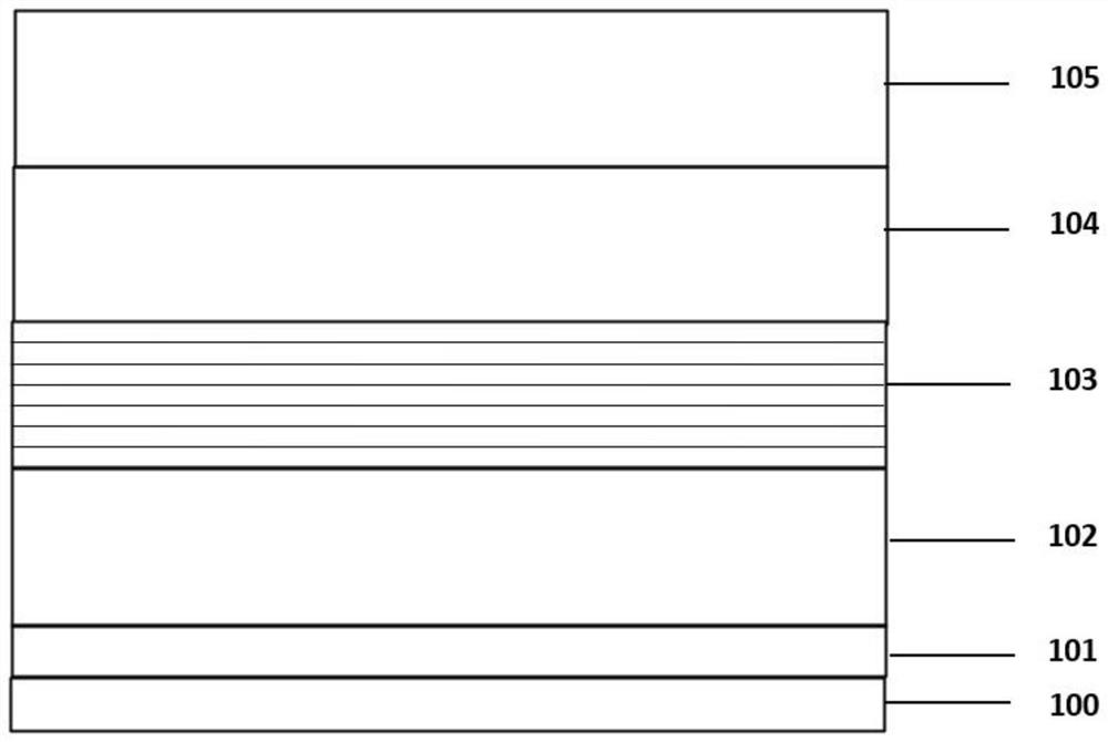
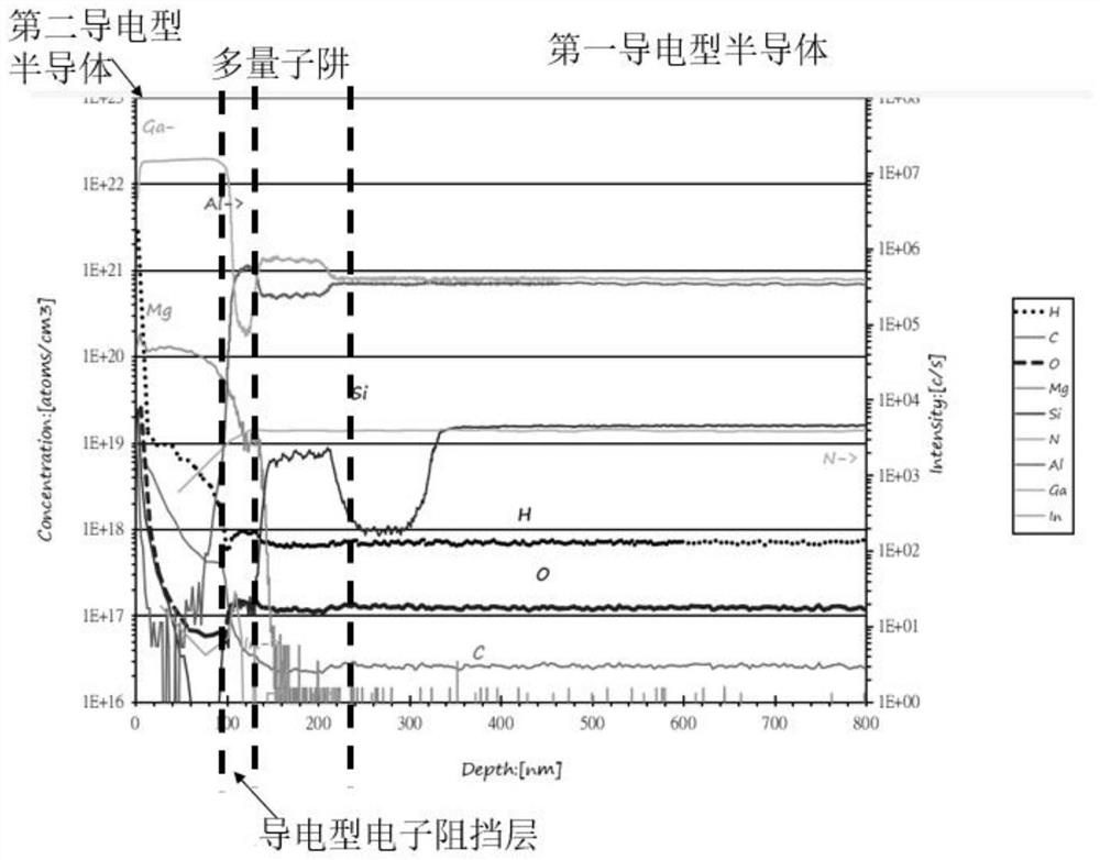
[0021] Such as figure 1 As shown, the deep ultraviolet semiconductor light-emitting element of Example 1 of the present invention includes, from bottom to top, a substrate 100, a buffer layer 101, a first conductivity type semiconductor 102, a multiple quantum well 103, a conductivity type electron blocking layer 104 and a second conductivity type semiconductor. type semiconductor 105, the substrate 100 is a substrate on which nitride semiconductor crystals can be epitaxially grown on the surface, and can be selected to meet the requirements for the wavelength range of light emitted by the semiconductor light emitting element. % or more) substrate; for example, as the mat...


PUM


Abstract

The invention relates to the technical field of semiconductor photoelectric devices, in particular to a deep ultraviolet semiconductor light-emitting element which sequentially comprises a substrate, a buffer layer, a first conductive type semiconductor, a multiple quantum well, a conductive type electron blocking layer and a second conductive type semiconductor from bottom to top, the H concentration of the conductive type electron blocking layer is 1E17-5E18cm <-3 >, the O concentration of the conductive type electron blocking layer is 1E17-1E18cm <-3 >, and the first conductive type semiconductor, the multiple quantum well, the conductive type electron blocking layer and the second conductive type semiconductor are sequentially arranged from bottom to top. By controlling the H / O content of the conductive electron blocking layer and regulating and controlling the H / O content and proportion suitable for the high-Al-component AlyGa1-yN material, the hole ionization energy of Mg in the layer can be effectively reduced, the hole ionization efficiency can be improved, and the free hole carrier concentration after ionization can be improved to 1E18cm <-3 > or above.

Description

technical field [0001] The invention relates to the technical field of semiconductor optoelectronic devices, in particular to a deep ultraviolet semiconductor light-emitting element. Background technique [0002] Semiconductor light-emitting elements have a wide range of adjustable wavelengths, high luminous efficiency, energy saving and environmental protection, can be used for more than 100,000 hours of long life, small size, strong designability and other factors; semiconductor light-emitting elements through the regulation of Al components, the wavelength The ultraviolet band can be as short as 200-350nm; high Al composition (Al composition greater than 40%) AlGaN material has low Al mobility, low lateral growth rate, and has a large lattice loss between AlGaN and sapphire substrate Allocation and thermal mismatch, resulting in the growth of high Al composition (Al composition greater than 40%) AlGaN materials is much more difficult than GaN materials and low Al composit...

Claims


Application Information

Patent Timeline
IPC IPC(8): H01L33/14H01L33/06H01L33/32
CPCH01L33/145H01L33/06H01L33/325
Inventor 王程刚
Owner 安徽格恩半导体有限公司
Features
  • R&D
  • Intellectual Property
  • Life Sciences
  • Materials
  • Tech Scout
  • Unparalleled Data Quality
  • Higher Quality Content
  • 60% Fewer Hallucinations
Learn More