Alignment mark for electron beam exposure and preparation method thereof
A technology of electron beam exposure and alignment mark, which is applied in the field of photolithography to achieve the effect of improving alignment accuracy and reliability
- Summary
- Abstract
- Description
- Claims
- Application Information
AI Technical Summary
Problems solved by technology
Method used
Image

Examples
Embodiment 1
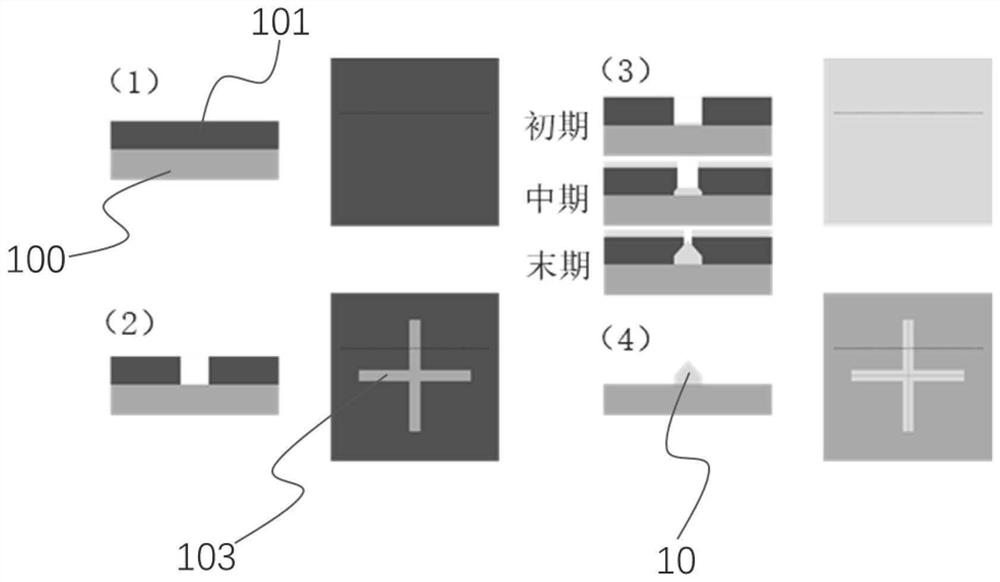
[0044] figure 2 A schematic flow chart showing the preparation of an alignment mark using a layer of photoresist according to an exemplary embodiment of the present application.
[0045] Such as figure 2 As shown, according to an exemplary embodiment of the present application, the present application discloses a preparation method of an alignment mark 10 for electron beam exposure, including: covering a photoresist 101 on a substrate 100; Expose and develop to remove a part of the photoresist 101 on the substrate 100, thereby forming a pattern with a predetermined shape; while depositing metal on the substrate 100 and the photoresist 101 remaining on the substrate 100, make The photoresist 101 on the substrate 100 is thermally expanded; and the photoresist 101 remaining on the substrate 100 and the deposited metal on the substrate 100 are removed, so that a deposited metal having a predetermined shape is obtained on the substrate 100 .
[0046] In other words, figure 2 ...
Embodiment 2
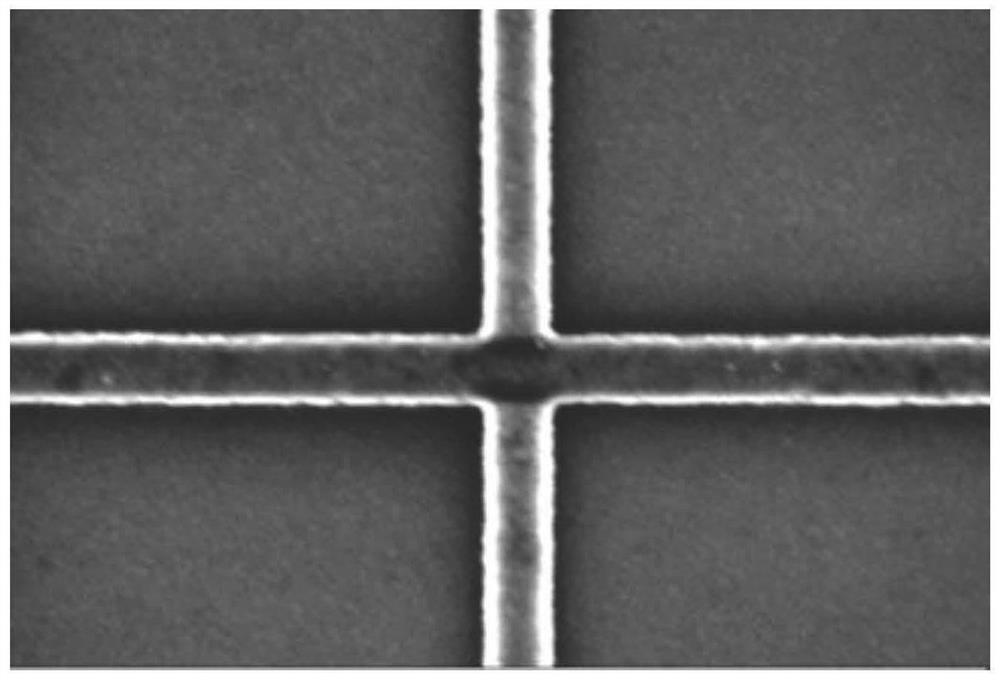
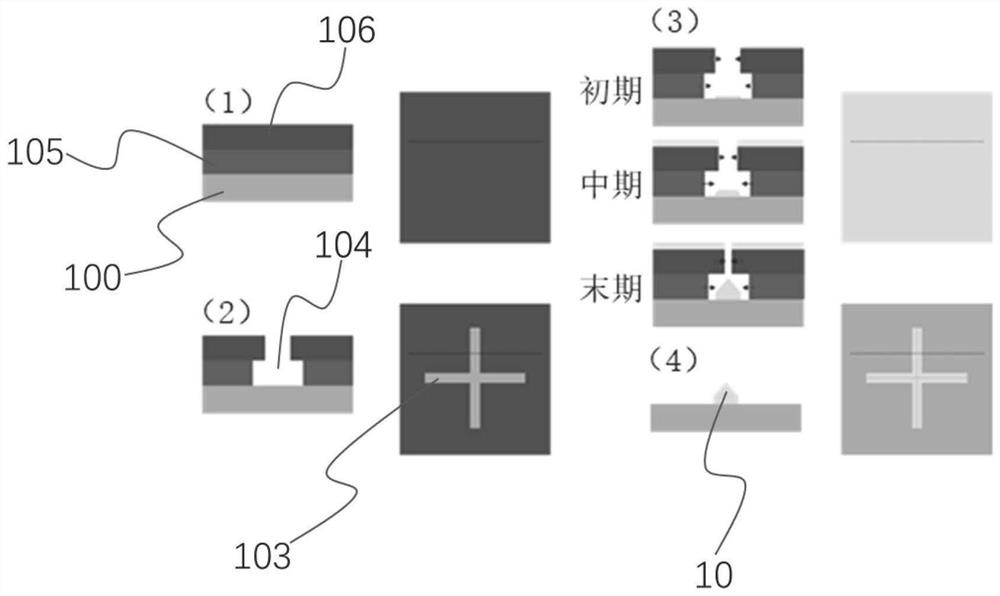
[0060] image 3 A schematic flow chart showing the process of preparing an alignment mark from a 2-layer photoresist according to an exemplary embodiment of the present application. Figure 4 A schematic diagram showing the electron microscope scanning structure according to an exemplary embodiment of the present application.
[0061] Such as image 3 As shown, according to one aspect of the present application, a method for preparing an alignment mark 10 for electron beam exposure is proposed, comprising: covering a first photoresist 105 on a substrate 100; Covering the second photoresist 106; exposing and developing the first photoresist 105 and the second photoresist 106 in a predetermined shape, so as to remove a part of the first photoresist 105 and a part of the second photoresist on the substrate 100 glue 106, thereby forming a pattern with a predetermined shape; while depositing metal on the substrate 100 and the second photoresist 106 remaining on the substrate 100,...
PUM
| Property | Measurement | Unit |
|---|---|---|
| Opening width | aaaaa | aaaaa |
Abstract
Description
Claims
Application Information
 - Generate Ideas
- Intellectual Property
- Life Sciences
- Materials
- Tech Scout
- Unparalleled Data Quality
- Higher Quality Content
- 60% Fewer Hallucinations
Browse by: Latest US Patents, China's latest patents, Technical Efficacy Thesaurus, Application Domain, Technology Topic, Popular Technical Reports.
© 2025 PatSnap. All rights reserved.Legal|Privacy policy|Modern Slavery Act Transparency Statement|Sitemap|About US| Contact US: help@patsnap.com